
NiCad charger with independent discharge


The problem with using such battery charger described partly addressed. After inserting the batteries, the batteries are discharged separately to the first voltage of 0.9 V and only then recharged. Can be recharged up to four AA (R6, "pencil article"). The smaller number of cells is one in which the position of an article is added, which remains empty. The first position is the backup status flip-flop circuits in a power failure, and therefore it should always be fitted article. Otherwise, the positions are completely equivalent. Charging is slow stream of slightly more than 0.1 C, but for most applications in the home does not matter. Stage-discharge cells can be easily omitted. Connecting the charger is on a separate page (Figure 1). The charger has a common source of reference voltage 1.25 V circuit LM317L (IO1), the timer circuit 4521 (IO6) and control the charging current (T9, PR1). Conversely discharging cycle is controlled for each article separately. After the insertion of articles and press the START button to reset the timer (IO6) signal on pin 2 (MR) and all of the RS flip-flops are set so that the output level H. The output of OR gate (IO5c, pin 10) is also a signal the level H, which blocked a signal to the timer pin 3 IO6 and rechargeable power source by opening the transistor T9. Diagram of a separate discharge circuit for an article on the figure 2. The first position of a current output of the RS flip-flop LED1 and resistor R9 to the base of transistor T2. The transistor T2 is opened and the battery is discharged current passing through resistor R1. The battery voltage is compared with a voltage comparator IO3 gained 0.9 divider R17, R18 of the reference source. Resistors R17 and R18 constitute both the minimum required load stabilizer and their resistance would not increase. Shrinks when the discharge voltage below 0.9 V battery, appears at the output voltage comparator, which resets the RS flip-flop and the discharge stops. At the same time LED1 extinguishes, indicating discharging. Discharging at the other positions is the same way. Articles are in fact the discharge voltage of slightly less than the output voltage divider R17, R18. The difference is caused by loss of the resistor R5, induced current flowing into the base of the transistor. Because this loss is very small (about 10 to 15 mV), has the function of the circuit virtually no effect. The output level H IO5c is so long until the discharge end of articles - then turns to L. The transistor T9 is closed and the batteries are charged at now, which is controlled by the voltage at the noninverting input IO2. The actual charging circuit for an article in Figure 3 At the same time LED5 also lights to indicate charging and enable timer IO6. Current sources are supplied from the transformer taps. At the turn of the transformer is half the supply voltage (half-wave rectification unit D1 diode), current consumption may be doubled. In this connection it is sufficient for proper function of current sources only a small voltage drop across the transistor - and reduces the power loss.
MOS integrated circuit 4521 includes 24stup?ový binary divider, the last 7 outputs is controllable, then OR gate, and somewhat uncharacteristically involved input circuits. OR gate inside the IC is connected to an input signal MR, the second entry gate is wired to the I1 (pin 9), O1 output (Pin 7). The charger is used for forming gate signal frequency of 50 Hz. The voltage from the secondary winding of the transformer is fed through resistor R24 to input I1. The output O1 is introduced hysteresis resistor R25. Signal with rectangular waveform is applied to the input I2 (pin 6). Outlets udd 'and USS' can be connected in various combinations on both the supply voltage. Then change the function of different input circuits and dividers, in one mode, the output is the entry even O2. For a more detailed description let candidates consult the catalog [2]. In that connection there is an input signal supplied from an output of the slicer input I2, gated voltage on pin Uss'. For proper use it is the O2 output (pin 4) connected through a resistor to a positive voltage.
Determination of charge is derived from the frequency of the network. If you do not want to complicate the timing circuit, it is advisable to choose the charging time, we derive a binary division. Used in the charger charging time period corresponds to 20 ms extended divider 2 ^ 21st After 11 hours and 39 minutes to appear Ø22 output signal with H, which is taken to the input OR gate (IO5b, pin 8). The output appears IO5c level H, and hang the timer and power supply. LED5 goes LED6 and lights up to indicate charging is completed. Accuracy of timer is more than sufficient. If we want the timer to control the crystal, we would add at least one integrated circuit such as 4060 in the capacity of the oscillator and divider. Timer-controlled RC oscillator would be set back.
Transistor T9 is never fully open. Because of its collector saturation voltage remains low, even after the articles charged, charging current of 1-2 mA. This "maintenance" current can vary at different positions, since at low voltage control current source has been fairly applied input voltage unbalance operational amplifiers. When power supply voltage is interrupted charging batteries being charged and no current is drawn. Status of the RS flip-flop circuits and binary divider, however, may change randomly. Therefore, it is complemented by the involvement of diode D2. Then, when a power failure at the first article of the position taken current about 1 mA, which supplies the control of the charger. The logic ICs, in this case a voltage of approximately 0.8 to 0.9 V, (as experience has shown) it is sufficient to maintain the status flip-flop circuits and timers.
The described battery charger is designed to manage the charging and discharging of multiple NiCad batteries with varying capacities and self-discharge rates. It features a separate discharge mechanism for each battery, ensuring that all cells are treated individually to prevent damage from over-discharge. The charger utilizes a LM317L voltage regulator to maintain a reference voltage and employs a timer circuit (IC 4521) to control the charging duration based on the frequency of the AC supply. Each battery is discharged to a safe voltage level of 0.9 V before being recharged, with the process managed by a series of flip-flops and transistors that control the flow of current. The charger is capable of handling up to four AA batteries simultaneously, with a dedicated position for a backup status indicator to ensure proper operation during power failures. The overall design emphasizes efficiency and safety, reducing the risk of damage to batteries while maximizing their lifespan through careful monitoring and control of the charging process.If you use different batteries with actual capacity, with different self-discharge rate of batteries from different manufacturers, you will perhaps throw further described charger. Because each cell can be discharged separately recharge, can be charged with varying articles carrying charge.
All of the described nabíjely NiCad battery chargers, or even be discharged all the articles (or group of cells) simultaneously. Such a charger is convenient to use if they are battery cells used in approximately the same capacity.
It is met only with new and very long in storage batteries and battery assembled modellers, who can work with a collection of articles. Collection of articles is quite time-consuming work, and so we, the other current users, we sort the batteries usually only criterion of good-bad. Then it may happen that one device will meet the batteries with different capacity and different self-discharge rate.
With the smallest capacity batteries suffer from the culling - are being discharged to zero voltage and sometimes even reverse polarity, thus significantly reduces the number of charge cycles and shortens their life. This danger is especially for batteries with more cells, which discharged a total of one article can not be easily distinguished from the perimeter indicating a slight discharge the entire battery.
The batteries have the greatest capacity on the contrary, according to the myths cherished memory effect manifests itself, since they usually are not charging the battery is completely discharged. The problem with using such battery charger described partly addressed. After inserting the batteries, the batteries are discharged separately to the first voltage of 0.9 V and only then recharged.
Can be recharged up to four AA (R6, "pencil article"). The smaller number of cells is one in which the position of an article is added, which remains empty. The first position is the backup status flip-flop circuits in a power failure, and therefore it should always be fitted article.
Otherwise, the positions are completely equivalent. Charging is slow stream of slightly more than 0.1 C, but for most applications in the home does not matter. Stage-discharge cells can be easily omitted. Connecting the charger is on a separate page (Figure 1) . The charger has a common source of reference voltage 1.25 V circuit LM317L (IO1), the timer circuit 4521 (IO6) and control the charging current (T9, PR1).
Conversely discharging cycle is controlled for each article separately. After the insertion of articles and press the START button to reset the timer (IO6) signal on pin 2 (MR) and all of the RS flip-flops are set so that the output level H. The output of OR gate (IO5c, pin 10) is also a signal the level H, which blocked a signal to the timer pin 3 IO6 and rechargeable power source by opening the transistor T9.
Diagram of a separate discharge circuit for an article on the figure 2 . The first position of a current output of the RS flip-flop LED1 and resistor R9 to the base of transistor T2. The transistor T2 is opened and the battery is discharged current passing through resistor R1. The battery voltage is compared with a voltage comparator IO3 gained 0.9 divider R17, R18 of the reference source.
Resistors R17 and R18 constitute both the minimum required load stabilizer and their resistance would not increase. Shrinks when the discharge voltage below 0.9 V battery, appears at the output voltage comparator, which resets the RS flip-flop and the discharge stops.
At the same time LED1 extinguishes, indicating discharging. Discharging at the other positions is the same way. Articles are in fact the discharge voltage of slightly less than the output voltage divider R17, R18. The difference is caused by loss of the resistor R5, induced current flowing into the base of the transistor.
Because this loss is very small (about 10 to 15 mV), has the function of the circuit virtually no effect. The output level H IO5c is so long until the discharge end of articles - then turns to L. The transistor T9 is closed and the batteries are charged at now, which is controlled by the voltage at the noninverting input IO2.
The actual charging circuit for an article in Figure 3 At the same time LED5 also lights to indicate charging and enable timer IO6. Current sources are supplied from the transformer taps. At the turn of the transformer is half the supply voltage (half-wave rectification unit D1 diode), current consumption may be doubled.
In this connection it is sufficient for proper function of current sources only a small voltage drop across the transistor - and reduces the power loss. MOS integrated circuit 4521 includes 24stup?ový binary divider, the last 7 outputs is controllable, then OR gate, and somewhat uncharacteristically involved input circuits.
OR gate inside the IC is connected to an input signal MR, the second entry gate is wired to the I1 (pin 9), O1 output (Pin 7). The charger is used for forming gate signal frequency of 50 Hz. The voltage from the secondary winding of the transformer is fed through resistor R24 ??to input I1. The output O1 is introduced hysteresis resistor R25. Signal with rectangular waveform is applied to the input I2 (pin 6). Outlets udd 'and USS' can be connected in various combinations on both the supply voltage. Then change the function of different input circuits and dividers, in one mode, the output is the entry even O2.
For a more detailed description let candidates consult the catalog [2]. In that connection there is an input signal supplied from an output of the slicer input I2, gated voltage on pin Uss'. For proper use it is the O2 output (pin 4) connected through a resistor to a positive voltage. Determination of charge is derived from the frequency of the network. If you do not want to complicate the timing circuit, it is advisable to choose the charging time, we derive a binary division.
Used in the charger charging time period corresponds to 20 ms extended divider 2 ^ 21st After 11 hours and 39 minutes to appear Ø22 output signal with H, which is taken to the input OR gate (IO5b, pin 8). The output appears IO5c level H, and hang the timer and power supply. LED5 goes LED6 and lights up to indicate charging is completed. Accuracy of timer is more than sufficient. If we want the timer to control the crystal, we would add at least one integrated circuit such as 4060 in the capacity of the oscillator and divider.
Timer-controlled RC oscillator would be set back. Transistor T9 is never fully open. Because of its collector saturation voltage remains low, even after the articles charged, charging current of 1-2 mA. This "maintenance" current can vary at different positions, since at low voltage control current source has been fairly applied input voltage unbalance operational amplifiers.
When power supply voltage is interrupted charging batteries being charged and no current is drawn. Status of the RS flip-flop circuits and binary divider, however, may change randomly. Therefore, it is complemented by the involvement of diode D2. Then, when a power failure at the first article of the position taken current about 1 mA, which supplies the control of the charger. The logic ICs, in this case a voltage of approximately 0.8 to 0.9 V, (as experience has shown) it is sufficient to maintain the status flip-flop circuits and timers.
🔗 External reference
Related Circuits
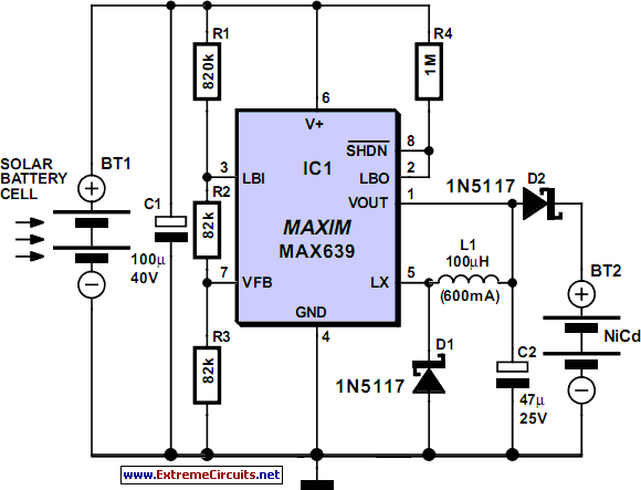
This is a simple NiCd battery charger powered by solar cells. A solar cell panel or an array of solar cells can charge a battery at more than 80% efficiency, provided the available voltage exceeds the fully charged battery...
This 24V to 36V linear battery charger is long overdue. While this is an old circuit technique, it is optimized for charging higher voltage lead-acid batteries. The 24V to 36V linear battery charger is designed to provide a stable charging...
The following circuit illustrates a simple battery charger equipped with a temperature sensor. This circuit is based on the LM350 integrated circuit. Features include negative... The circuit utilizes the LM350 voltage regulator IC, which is known for its ability to...
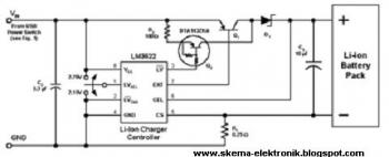
This circuit is designed to charge NiCad battery packs within the voltage range of 4.8 to 15.6 V using a convenient remote power source, such as an automobile battery. Upon initial power application, a small bias current supplied by...
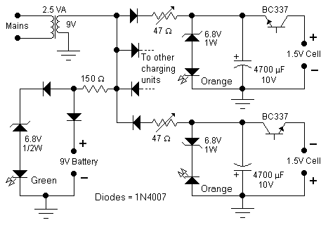
Alkaline Battery Charger. This circuit was specifically designed to recharge alkaline cells. The unusual connection of the transistor in each charging unit will cause it to oscillate. The alkaline battery charger circuit is engineered to effectively recharge alkaline batteries, which...
This automatic battery charger circuit is ideal for charging batteries used in alarm systems that require battery buffering. Caution must be exercised when connecting the battery to ensure correct AC polarity. It is essential to meticulously follow the schematic...