
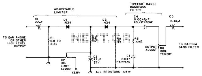
Noise limiter

The limiter circuit operates by controlling the amplitude of the signal passing through it, effectively reducing the noise level while preserving the integrity of the desired audio signals. The placement of the limiter is crucial; it should be positioned between the output of the detector and the input of the audio stage to ensure optimal performance. The high-impedance nature of the connection helps to prevent loading effects that could distort the audio signal.
In this configuration, diodes D1 and D2 play a significant role. Their low forward resistance allows them to conduct when the signal exceeds a certain threshold, effectively clamping the signal to prevent it from exceeding this limit. The high reverse resistance ensures that the diodes do not conduct during negative cycles of the audio signal, thereby maintaining the integrity of the audio waveform.
The choice of capacitor C1 is also critical. Increasing its value will allow the circuit to function effectively with receivers that have narrower bandwidths, which typically require better signal conditioning to minimize distortion and maintain clarity. The overall design of this limiter circuit is tailored to enhance the performance of audio receivers, particularly in environments where signal-to-noise ratios are a concern, ensuring that the output maintains a high level of fidelity despite the presence of noise.This limiter improves signal-to-noise ratio. It is connected between the detector output and the audio input (if high impedance) or at some relatively high-impedance section between two audio stages—preferably the low level stages.D1 and D2 can be any diode having relatively low forward resistance and very high back resistance. The circuit is excellent for receivers having bandwidths down to 2 or 3 kHz. Increase the value of Cl for receivers having narrower bandwidths.
Related Circuits
This circuit employs a diode series clipper to limit noise peaks on a received signal. It is most effective in scenarios where several volts peak-to-peak of audio signal are present. The diode series clipper circuit is designed to protect subsequent...
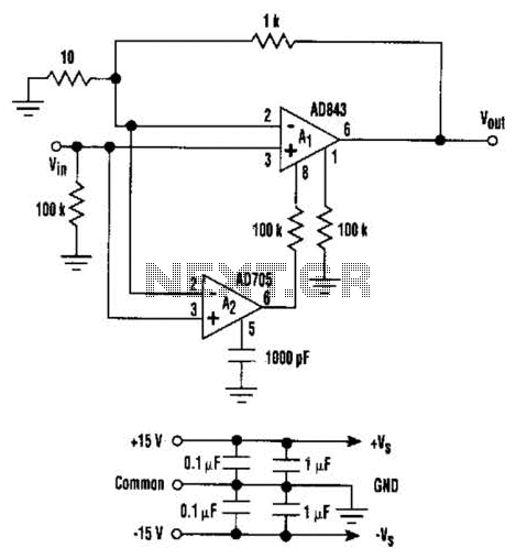
This circuit combines the advantages of low input offset voltage and drift without compromising the overall dynamic performance of the system. When compared to a standalone FET input operational amplifier, the composite amplifier circuit demonstrates a 20-fold improvement in...
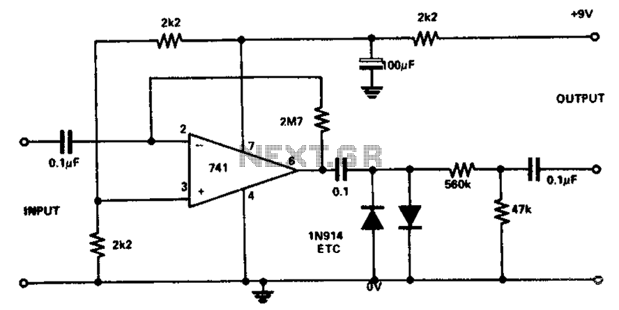
The circuit utilizes the 741 operational amplifier, which has a maximum gain of 20,000. However, the design achieves a gain of 2.7 million, resulting in output distortion. This distortion is attributed to noise effects. Two clamping diodes are employed...
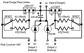
This is an advanced version of a basic charge rate limiter that allows for the simultaneous charging of two battery packs from a single wall charger. For detailed circuit descriptions and parts lists, refer to the simple charger page....
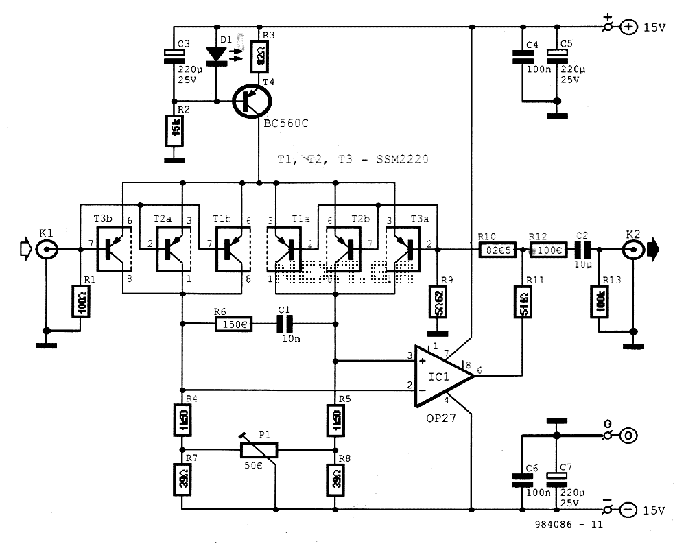
The preamplifier is designed for signal sources such as low-impedance moving coil cartridges (MC) used in high-fidelity turntables. The amplifier has an impedance of 100 ohms. To maintain low noise levels, three double-type transistors, either MAT03 or SSM2220, are...
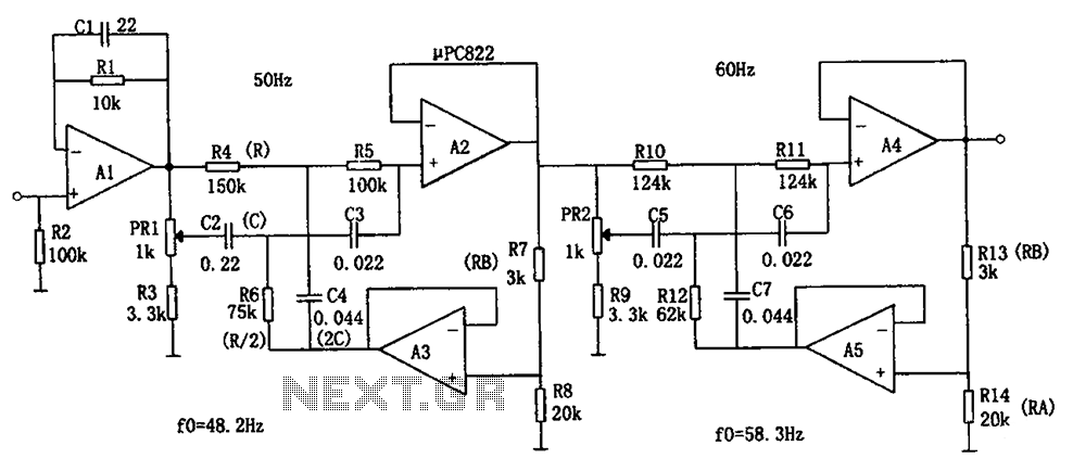
The circuit depicted in the figure is a frequency power supply noise filter circuit, specifically a double-T filter. It is designed to amplify weak signals, such as those from sensors, while filtering out mixed 50Hz (or 60Hz) power supply...