
oscillator

The Colpitts oscillator is a type of electronic oscillator that generates sinusoidal waveforms using a combination of inductors and capacitors in its tank circuit. The oscillator relies on the principle of positive feedback to sustain oscillations. The tank circuit, which comprises the two capacitors (C1 and C2) and the inductor (L1), determines the oscillation frequency, which can be calculated using the formula:
\[ f = \frac{1}{2\pi\sqrt{L \cdot C_{total}}} \]
where \( C_{total} \) is the equivalent capacitance of C1 and C2 in series, given by:
\[ C_{total} = \frac{C1 \cdot C2}{C1 + C2} \]
The resistors R1, R2, R3, and R4 are crucial for biasing the transistor and ensuring stable operation. R1 and R2 form a voltage divider that sets the base voltage, while R4 provides the necessary emitter bias. Resistor R3 not only loads the collector but also facilitates feedback to the tank circuit, influencing the amplitude of oscillations.
The transistor Q1 is typically operated in Class A mode, allowing for continuous conduction. When the circuit is powered, the initial conditions lead to capacitor C1 charging and discharging, establishing the oscillation process. The interaction between the capacitors and the inductor creates resonant conditions that sustain the oscillations.
The Colpitts oscillator is widely used in RF applications, signal generators, and various communication systems due to its relatively simple design and ability to produce stable frequencies. The careful selection of component values is essential for achieving the desired frequency response and minimizing distortion.Circuit Colpitts Oscillator schematics Circuit Electronics, Colpitts oscillator is very similar to the shunt-fed Hartley oscillator. The principal difference is in the tank circuit. In the Colpitts oscillator, two capacitors are used as replacement coils are divided. Basic oscillatorFeedback oscillator colpitts developed using the "electrostatic field" through the capacitor divider network. Colpitts oscillator frequency is determined by two capacitors connected in series and inductors. Voltage to the base provided by R1 and R2 while for emiitor given by R4. Collector voltage given back by connecting to the positive part of the VCC through R3. This resistor (R3) also functions as a collector load. Transistor is connected with the emitter-joint configuration. When the DC power supplied to the circuit, current flows from the negative part of V CC through R4, Q1 and R3. IC currents flowing through R3 causes a decrease in the voltage VC with a positive price. voltage changes to negative direction are supplied to the top of the C1 through C3. The lower part of C2 positively charged and the voltage flowing to the base voltage so that the IB price rises.
Transistors Q 1 will increasingly berkonduksi until the saturation point. When Q 1 to the saturation point there was no increase in IC and VC changes will also be halted. There is no feedback to the C2. Magnetic fields C1 and C2 will be disarmed through the L1 and the subsequent magnetic field around it will disappear. Emptying flow persists for a moment. C2-chip bottom becomes negatively charged and pieces of the upper positively charged C1. This will reduce the forward voltage of Q 1 and the IC will be decrease. Price V C will begin to rise. This increase will be fed back to the top of the chip C1 through C3. C1 will charge more positive and the bottom of the C2 becomes more negative. This process continues until Q 1 to the cutoff point. When Q 1 to the cutoff point, no current I C. No feedback voltage to the C1. Combined charge collected on the C1 and C2 stripped through L1. Currents flowing from the bottom of disarmament to the top of C1 C2. C2 negative charge will eventually run out and the magnetic field around L1akan disappeared. Currents that flow continues. C2 puck into the lower positive charge and the chips C1 upper negative charge. Positive voltage on C2 interesting Q 1 of the cutoff region. Furthermore, the IC will begin to flow again and the process starts again from this point. capacitance "C1 and C2. The price of C1 in this circuit is much smaller than the C2 or C1 X> X C2. The voltage on C1 is greater than C2. By creating a smaller C2 would obtain feedback voltage is greater. But by raising the feedback too high will cause distortion. Usually around 10-50%, the collector voltage is returned to the tank circuit as a feedback. 🔗 External reference
Related Circuits
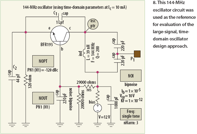
Unlike conventional small-signal methods, employing large-signal, time-domain design techniques facilitates the creation of low-noise grounded-base oscillators suitable for VHF/UHF applications. The development of low-noise grounded-base oscillators for VHF/UHF applications presents unique challenges and opportunities. By utilizing large-signal, time-domain design techniques,...
Assistance is required for the design of a FET-based Wien bridge oscillator and its simulation using PSpice. Any suggestions would be appreciated. The Wien bridge oscillator is a type of electronic oscillator that generates sine waves. It employs a bridge...

Inquiries about selecting the L, C, and R values to achieve a desired frequency are common. It is essential to understand the relationship between these components and the frequency they produce. The desired frequency can be calculated using the...

A discrete oscillator circuit illustrated in the schematic diagram below is a variable duty cycle and variable frequency oscillator, which can be utilized to generate various output waveforms. The discrete oscillator circuit is designed to produce oscillations with adjustable frequency...
A voltage-controlled oscillator (VCO) is an electronic signal generator that produces a signal with a variable frequency, which is dependent on an input voltage level. A voltage-controlled oscillator is a fundamental component in various electronic applications, including phase-locked loops (PLLs),...

This oscillator may contain several switched crystals to provide channelized operation. A buffer amplifier may be added if desired. The oscillator described is designed to utilize multiple switched crystals, enabling it to operate across various frequency channels. This feature is...
Warning: include(partials/cookie-banner.php): Failed to open stream: Permission denied in /var/www/html/nextgr/view-circuit.php on line 713
Warning: include(): Failed opening 'partials/cookie-banner.php' for inclusion (include_path='.:/usr/share/php') in /var/www/html/nextgr/view-circuit.php on line 713