
Frequency Divider

The described frequency divider circuit utilizes three 7490 decade counters (IC1, IC2, and IC3) configured in a cascading arrangement to achieve a division ratio of up to 999. Each 7490 counter is capable of counting from 0 to 9, and when cascaded, they effectively form a binary coded decimal (BCD) counter. The input signal, a TTL compatible square wave, is fed into the first counter (IC1), which increments its count with each pulse. As the count progresses through the three counters, the total count is represented in BCD format.
Once the cumulative count reaches the predetermined division ratio, all outputs of the fourth integrated circuit (IC4), which is a 7430 NAND gate, will transition to a high state. This state change causes the output of IC4 to drop low, which serves as a trigger for the monostable multivibrator formed by IC5B and IC5C. The output pulse generated by this monostable multivibrator is short, effectively resetting the counters by driving the output of IC5A high. This reset allows the counting process to restart, enabling continuous frequency division.
To program the circuit for a specific division ratio, the BCD equivalent of the desired ratio must be calculated and set on the inputs of the counters. For instance, a division ratio of 569 would require the BCD representation of 5 (0101), 6 (0110), and 9 (1001) to be applied to the corresponding inputs of the counters. It is important to note that not all division ratios are feasible; for example, a division ratio of 777 cannot be achieved with this configuration due to the limitation of only having 8 inputs available for IC4.
The circuit also includes passive components such as a 680-ohm resistor (R1) and a 100 pF ceramic capacitor (C1) for timing and stability purposes, along with a 1 kΩ resistor connected to the unused inputs of IC4 to pull them to a high state (5V). This ensures that the circuit operates correctly within the specified voltage levels for TTL logic.This circuit will divide the frequency of a TTL compatible square wave signal by a factor from 0 to 999. The circuit comprises three decade counters IC1 to IC3 and a few NAND gates. The three 7490?s are cascaded and count is the input signal. When the desired and count reached all the inputs of IC4 become high, so the output goes low. This triggers the monostable consisting of IC5B and IC5C, which provides a sort output pulse. The output of IC5A goes high, resetting the three counters and the count then begins again. To program the counter it is first necessary to work out the binary coded decimal (BCD) equivalent of the required division ratio.
In the example shown the division ratio is 569. The unused inputs of IC4 are connected to +5V via a 1K resistor. Note that the circuit will not divide by 777, since this would require 9 inputs to IC4 and only 8 are available. R1=680 ohms C1=100pF ceramic IC4=7430 R2=1 Kohms IC1-2-3=7490 IC5=7400 🔗 External reference
Related Circuits
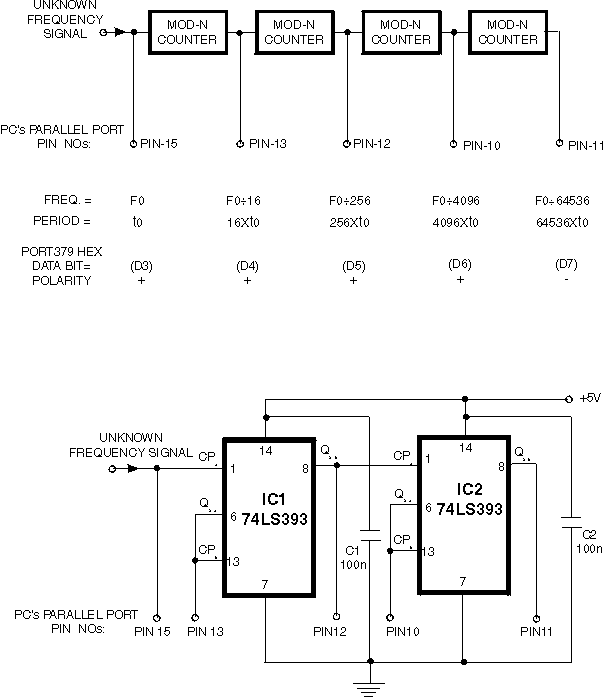
A technique for measuring frequencies across a wide range with acceptable accuracy using a PC is described. This method involves measuring the period of a complete wave at low frequencies to calculate frequency from the measured time period. Cascaded...
Current negative feedback voltage divider biased circuit diagram. The current negative feedback voltage divider biased circuit is a configuration commonly used in electronic amplifiers to stabilize the operating point and improve linearity. This circuit typically consists of an amplifier, a...
Apply a signal to each differential amplifier input pair. When the gate voltage changes from one extreme to the other, the output can alternate between the two input signals. When the gate level is high (1.5 V), a signal...

The meter will display the frequency from a power generator. Incoming sine waves are transformed into square waves by the 100K resistor and the 6.8 V zener diode. The square wave is differentiated by the capacitor, and the current...

The CYWUSB6953 is a comprehensive Radio System-on-Chip (SoC) device that facilitates the implementation of various simple RF systems using a single chip and a few discrete components. It is specifically designed for low-cost wireless systems that operate within the...
As shown in figure 14-17, this circuit consists of the input circuit, the line frequency synchronization generator, the sample-and-hold circuit, the voltage control delay generator, and the RF modulator. The input circuit includes the input attenuator RP1 and the...