
Basic reference bias circuit transistor - negative voltage feedback
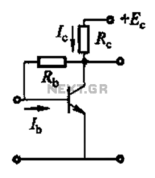
The basic reference bias circuit utilizing a transistor with negative voltage feedback is designed to provide a stable output voltage or current that is largely independent of variations in temperature and power supply. The circuit typically consists of a bipolar junction transistor (BJT) configured in a feedback arrangement, where a portion of the output is fed back to the input to maintain stability.
In this configuration, the transistor operates in the active region, where it can amplify the input signal. The negative voltage feedback is achieved by connecting a resistor from the output to the base of the transistor. This resistor forms a voltage divider with the base-emitter junction, effectively reducing the base voltage as the output voltage increases, which in turn decreases the collector current. This feedback mechanism stabilizes the output by counteracting any changes in the load or supply voltage.
The circuit may also include additional components such as capacitors for filtering and resistors to set the biasing conditions. The use of bypass capacitors can help to filter out high-frequency noise, ensuring a clean and stable reference voltage. The values of the resistors and capacitors must be carefully selected to achieve the desired response time and stability of the circuit.
Overall, this basic reference bias circuit is essential in various electronic applications where a reliable and constant reference voltage is required, such as in amplifiers, oscillators, and other analog circuits. It serves as a foundational element in designing more complex electronic systems. Basic reference bias circuit transistor - negative voltage feedback
Related Circuits
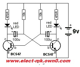
Robot eyes circuit of Service. A simple circuit to simulate a man appointed to it. It consists of a dual-lamp working in an unsteady manner. Circuit diagram. The robot eyes circuit is designed to create a visual effect that simulates...
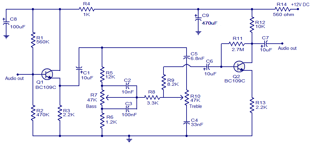
This simple tone control circuit is designed based on the renowned Baxendall tone control circuitry. The circuit can provide a maximum cut or boost of approximately 12 dB at both 10 kHz (treble) and 50 Hz (bass). Additionally, both...
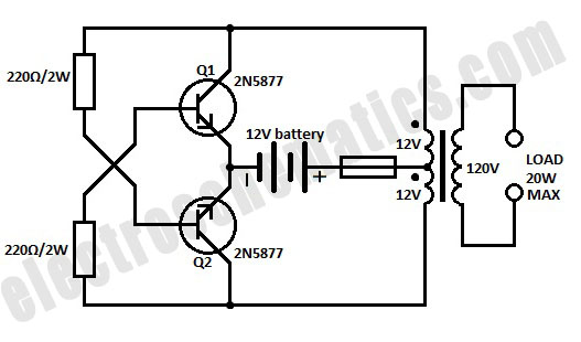
A simple 12-volt inverter circuit. This 120V AC power source is constructed using a basic 120V:24V center-tapped control transformer and four additional components. The circuit generates a clean 200-V peak-to-peak square wave at 60 Hz and is capable of...
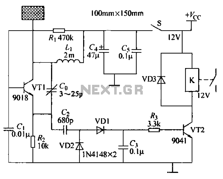
A capacitive proximity controller typically consists of a radio frequency oscillation circuit and a detection plate. The circuit is constructed using discrete components for capacitive proximity sensing detection. The transistor VT1, along with surrounding components, forms a radio frequency...

This simple water detector circuit utilizes alternating voltage to prevent electrode corrosion. It is easy to construct and employs N1 as a trigger Schmitt gate to generate the AC signal. When a conductive substance, such as an aqueous solution,...

This system utilizes an MM5369 integrated circuit (IC) to generate a 60 Hz signal from a television burst crystal operating at 3.579 MHz. The components F8 and V9 produce 10 Hz and 1 Hz signals derived from the 60...