
Overview of the MSP430 Microcontroller from Texas instruments

MSP430 device documentation is categorized into three main types: device-specific data sheets (e.g., MSP430G2553 data sheet), family user guides (e.g., MSP430x2xx family user guide), and device-specific errata sheets (e.g., MSP430G2553 device errata sheet). The data sheet includes essential information such as pinouts, block diagrams, operating conditions, electrical parameters, and performance tolerances. The family user guide encompasses details applicable to all devices in a family, including peripheral descriptions and CPU instruction sets. The errata sheet highlights any known device bugs and potential workarounds. All relevant documents, including application notes, example code, and development tool documentation, can be accessed through the device-specific product folder (e.g., MSP430G2553 product folder). The front page of the data sheet summarizes key aspects of the device, including power consumption, clock capabilities, and peripheral options, serving as an introductory overview. However, a deeper examination of the data sheet is necessary to fully understand the device's capabilities and limitations, including the available device variants, which differ in flash or RAM size, peripheral availability, I/O support, and package options. Prioritizing specific areas of the data sheet is recommended for a thorough evaluation of an MSP430 MCU.This module gives a brief overview of the MSP430 microcontroller, how to read a data sheet for an MSP430 microcontroller, and how to pick the right one for some sample applications. This module is one of many in a textbook designed to help seniors select TI products for use in their senior project.
MSP430 microcontrollers (MCUs) from Texas Instruments are 16-bit, RISC-based, mixed-signal processors designed specifically for ultra-low power. MSP430 MCUs have the right mix of analog and digital integrated intelligent peripherals, ease of use, low cost and lowest power consumption for thousands of applications ranging from simple sensor designs to complex electricity meters.
To get a better idea of what the MSP430 MCU is and how you can use it to solve a system design need or application problem, let`s take a look at a typical block diagram for a device. Figure 1 is the device block diagram for the MSP430G2553, one of the MSP430 Value Line devices. The purpose of the block diagram is to provide a high-level reference of the integration and feature set found in a given device.
You can find the block diagram for any MSP430 MCU in the data sheets at The block diagram contains key features of the device that can help you quickly identify if an MSP430 MCU is a fit for a given application need. There are a few features you will need to consider: USCI (A0/B0): universal serial communication interface module capable of providing standard UART, SPI and I2C communication protocols used to interface with external digital devices (sensors, data converters, radio ICs).
Figure 2 is the corresponding pinout also found in each device data sheet for the MSP430G2553. Here you can see exactly how peripheral functions are mapped onto the multiplexed I/Os of the device. Each I/O pin can be configured in software to provide the desired pin function for a given I/O based on its internal connectivity.
Figure 2 also shows the necessary power-supply connections (DVCC, DVSS), programmer/debugging tool connections (SBWTCK, SBWTDIO), and general I/O and peripheral connections (P3. 1, TA1. 0, CA2, UCB0SDA). When beginning any design with the MSP430 MCU, reviewing the given device`s block diagram and package pinout can provide a great guide to what is possible, as well as any constraints (such as memory size or pinout limitations).
Connecting the MSP430 MCU in any system is, in most cases, very straightforward. The first consideration should be the power-supply requirements. Most MSP430 devices operate at 1. 8 V to 3. 6 V, so a typical 3-V supply will work great. Connecting the JTAG to support device memory programming and debugging is also important. For MSP430G2xxx devices, there are two possibilities: standard four-wire JTAG or MSP430 MCU-specific Spy-Bi-Wire (SBW, or two-wire JTAG). Both interfaces are acceptable for programming and debugging application code. The main advantage of the four-wire mode is speed. The main advantage of the two-wire SBW mode is reduced pin-connection requirements. Figure 3 is an example schematic thatshows the baseline connections for the MSP430G2553, as well as some examples of other connections that can be made to the I/Os and integrated peripherals.
Figure 3 shows the connections of the MSP430G2553 in a typical sensor interface application. In this example, the MSP430G2553`s integrated ADC10 is used to measure an analog signal via a thermistor that changes resistance as temperature increases or decreases, and also interfaces using an I2C bus from the USCI module to an external humidity sensor. In addition, a 32. 768-kHz watch crystal keeps accurate timing; two switches, along with one PWM-controlled LED, provide a simple user interface.
To save power from the 3-V coin cell battery, when not in use the humidity sensor and thermistor ladder can be powered off using a general-purpose I/O (P2. 5) and the internal voltage reference (VREF+), respectively. Now that we`ve covered the basics and how to understand the capabilities of a given MSP430 device, let`s look more closely at the documentation and how to use it most effectively.
MSP430 device documentation can be broken up into three main categories: Device-specific data sheet (e. g. , MSP430G2553 data sheet. ) Here, you will find anything device-specific: pinouts, block diagrams, absolute operating conditions (supply voltage and operating temperature ranges), electrical parameters and performance tolerances (power consumption, ADC accuracy, and internal clock minimum and maximum frequencies).
Device family user`s guide (e. g. , MSP430x2xx family user`s guide). This document contains information applicable to all devices in a family: peripheral detailed descriptions, register and bit function definitions, CPU and instruction set, power mode definitions and settings. Some peripherals included in the user`s guide will not be present in a given device, as it is intended to cover all peripherals within a given family.
Device-specific errata sheet (e. g. , MSP430G2553 device errata sheet). The errata sheet is a critical document that lists any device bugs that can affect a given use-case along with potential workarounds. Errata can vary by device as well as device revisions. You can find these documents, as well as additional reference material such as application notes, example code and development tool documentation, by navigating to the device-specific product folder (e.
g. , MSP430G2553 product folder). Here, you can find the latest information as well as links to all pertinent documentation and software to aid your design efforts. Arguably, the most valuable document is the device-specific data sheet. We have already looked at two core aspects (pinout and block diagram), but let`s dive a bit deeper into the information provided.
The front page of the data sheet is designed to highlight all of the key aspects of the device organized into bulleted lists (Figure 4). It is comprehensive, showing typical power consumption, clock system capabilities, peripheral mix and package options.
This information is a great start, but is targeted as more of a marketing message than a reference. Going beyond the first page is critical to fully assess the given device`s capabilities and its limitations. Looking beyond the first page begins to yield the information needed to really design a system with the MSP430 MCU.
This begins with the available options for the device and variants. For example, there are 40 device and orderable part number variants for the MSP430G2553 device. These variants provide different mixes of flash or RAM, peripherals available, number of I/Os supported, and package options such as DIP or surface-mount options. While all information in a data sheet should be considered important, we recommend focusing on these areas when reviewing a data sheet for a specific MSP430 MCU.
🔗 External reference
Related Circuits
Build a large dancing robot. This was intended to be a walking robot, but it ended up moving in a more rhythmic manner. A video is available in the last step. The project involves the construction of a large dancing...

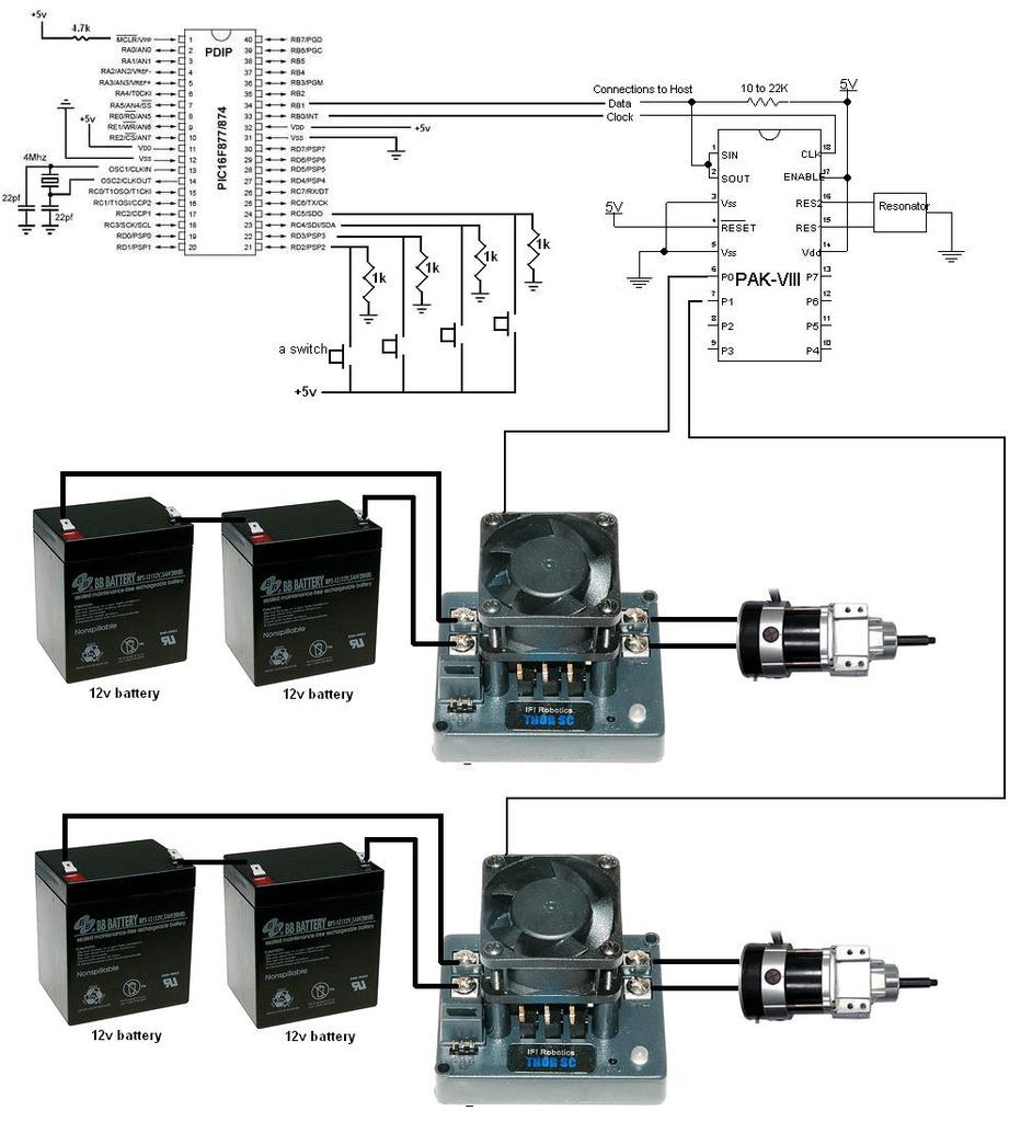
Both specifications were contradictory; a large display would require a significant amount of power, while the intention was to use the smallest battery for the longest duration. The solution was to separate the power supply for the logic and...

A USB solution is required for a project utilizing the LPC2148 microcontroller (MCU). In the past, interfaces such as LPT or COM were commonly used to connect projects to a PC, but these have become obsolete. The project allows...
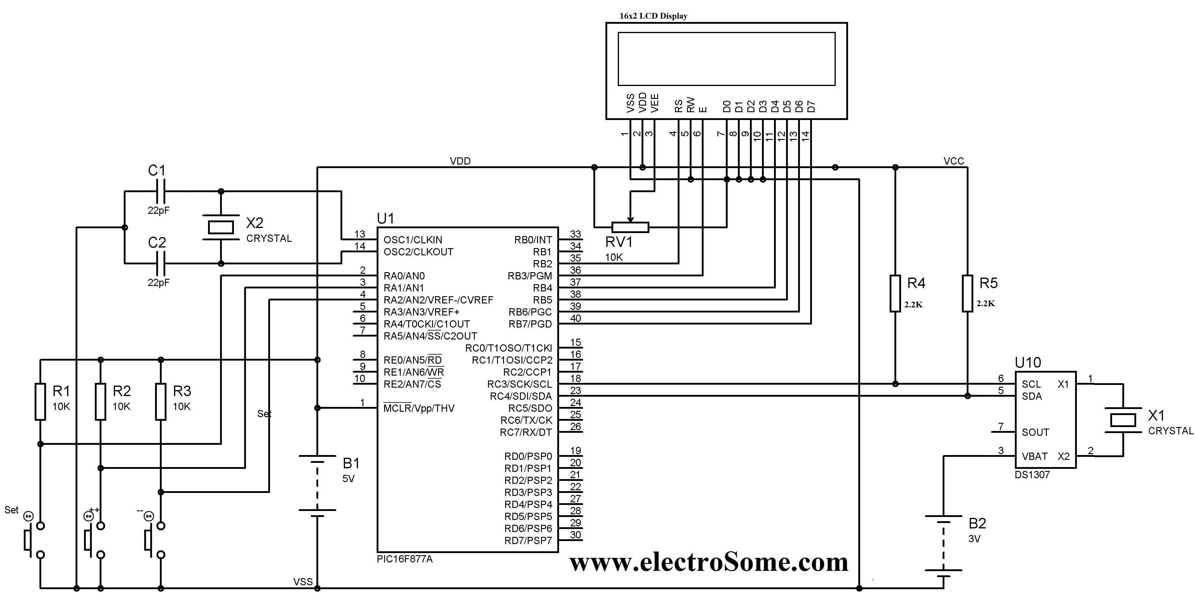
A digital clock can be constructed using a PIC microcontroller, DS1307 real-time clock (RTC), and a 16x2 LCD display. The DS1307 RTC operates in either 24-hour or 12-hour mode with an AM/PM indicator. It adjusts automatically for months with...

An NPN bipolar transistor is typically utilized for relay switching, particularly with 12V coil-rated relays, as it helps maintain circuit separation. A diode is also added to prevent issues. The necessity of driving the relay with a transistor depends...
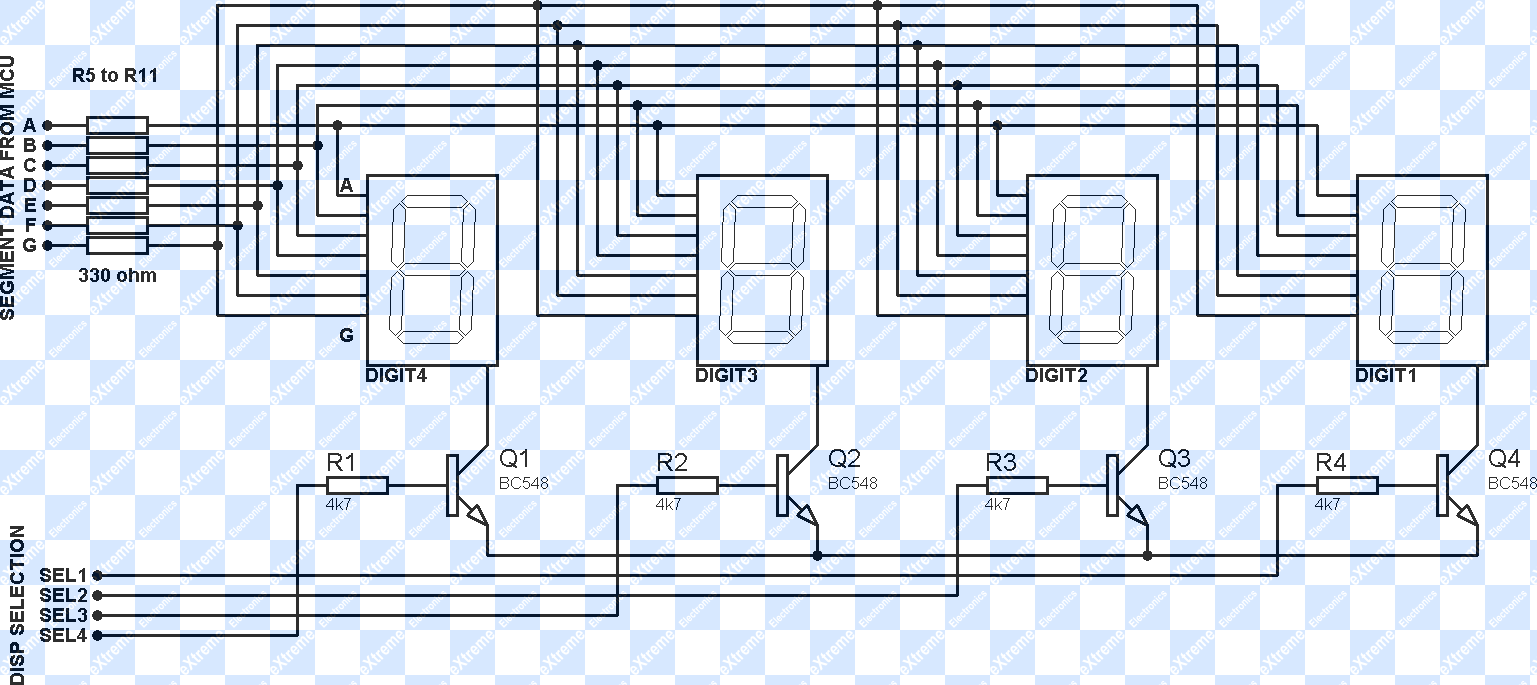
The project involves displaying the current room temperature using an LM35 temperature sensor. This schematic differs from a previous schematic that utilized a multiplexed seven-segment display. In the earlier schematic, the display select I/O pins were RA0, RA1, RA2,...