
passive pfc circuit cuts inductor value and size

Passive power factor correction circuits are utilized to improve the power factor of electrical systems by reducing the phase difference between voltage and current. In these circuits, the input current remains stable even when there are fluctuations in output ripple, which is the residual periodic variation in DC voltage. This characteristic allows for the design of circuits that require less inductance, thereby simplifying the overall circuit topology and potentially reducing costs and physical size.
The operation of a passive PFC circuit typically involves the use of inductors and capacitors to filter and smooth the input current. The reduced requirement for inductance means that smaller inductors can be employed, which can lead to a decrease in core losses and improved efficiency. Additionally, smaller inductors can facilitate a more compact design, making the circuit suitable for applications where space is limited.
When designing a passive PFC circuit, careful consideration must be given to the selection of components, including the inductor and capacitor values, to ensure that the circuit meets the desired performance specifications. It is also important to analyze the impact of load conditions and variations in supply voltage, as these factors can influence the overall effectiveness of the PFC circuit.
In summary, the insensitivity of input current to output ripple in passive PFC circuits allows for the implementation of smaller inductance, contributing to enhanced efficiency and a more compact design. This advancement represents a significant improvement over previous circuit designs, making passive PFC circuits a valuable solution in modern power electronics.Input current for a passive PFC circuit is insensitive to changes in the output ripple - so it requires a smaller inductance than previous circuits.. 🔗 External reference
Related Circuits
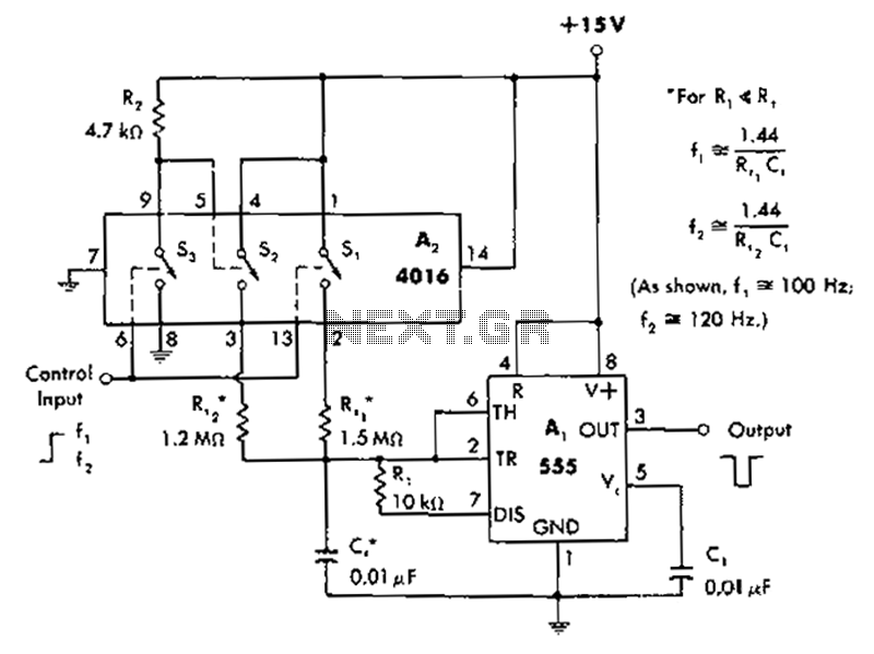
A circuit diagram controls the timing based on the input line state. When the input line is high, the 4016 CMOS analog switches select the timing of a 1.5 megohm resistor (Rt1) to produce negative output pulses at a...
The circuit consists of two discrete PNP Darlington transistors that form the external PNP transistor QEXT circuit to enhance output current. The use of integrated Darlington transistors is not recommended, as the internal base-emitter resistor can introduce additional errors....
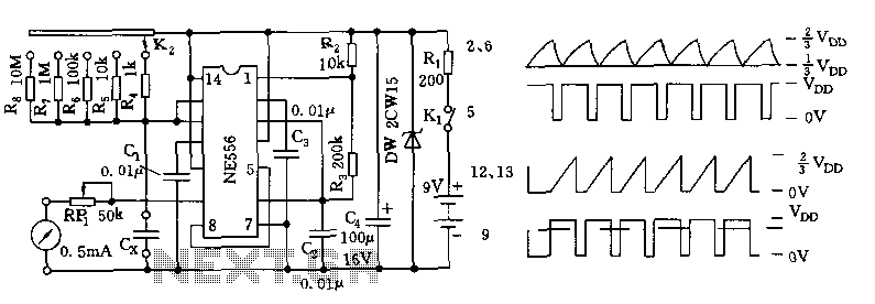
The tester comprises a dual time base circuit using a 556 timer and various RC components. The right side of the circuit features the 556 timer (556 1/2) along with resistors R2, R3, capacitors C2, C3, and additional components...
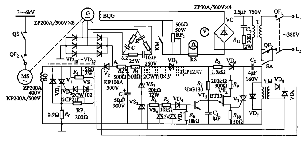
The circuit depicted in Figure 16-105 illustrates a synchronous motor. The components include BQ, which represents its field winding, and G, which denotes the AC excitation for the motor. The notation BQG indicates the field winding, with an empty...

The LM317 integrated circuit (IC) is commonly recognized as a voltage regulator; however, it can also function as an audio amplifier. This low-power amplifier circuit designed with the LM317 provides a maximum output of approximately 1 watt. The LM317...
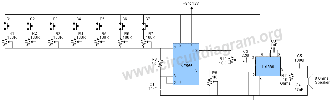
This schematic illustrates a simple 555 organ circuit, which consists of two main components: the 555 timer circuit that generates tones and an LM386 amplifier for driving an 8-ohm speaker. The circuit produces slightly different tones when each switch,...