
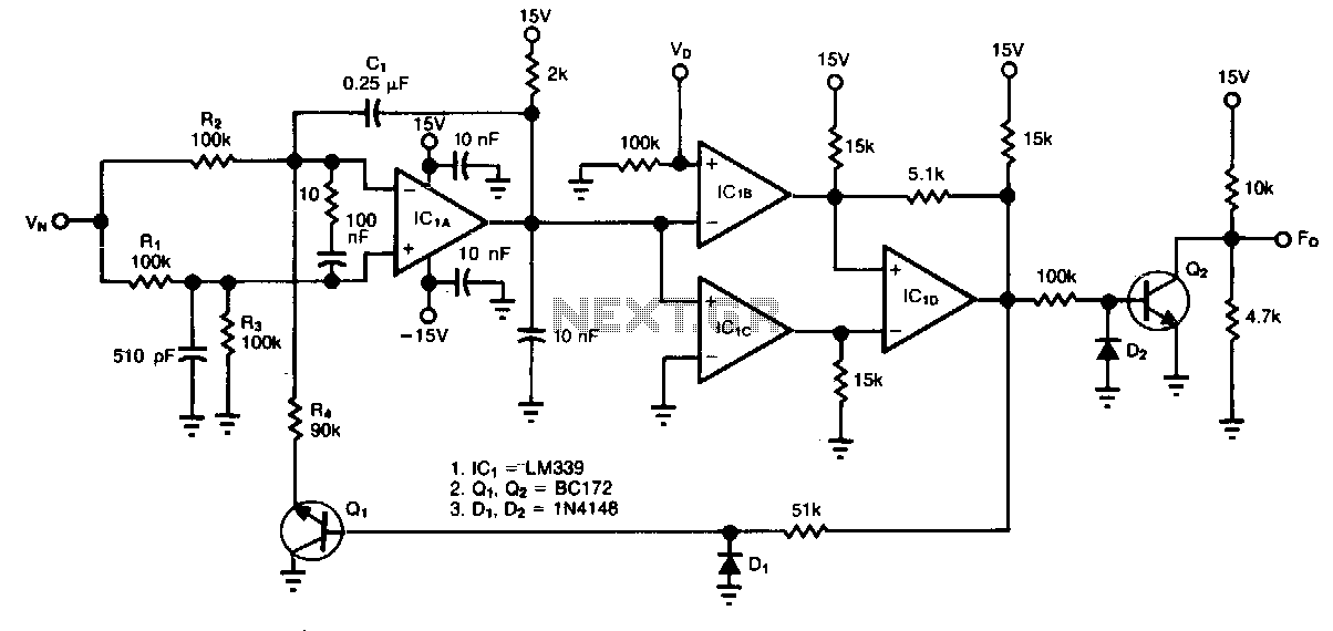
Period-To-Voltage Converter

The circuit described involves multiple components working in conjunction to process an input signal effectively. The input signal is applied to the ICD, which has a positive input offset of +0.1 V, resulting in a steady-state output voltage of approximately +13 V. This output is critical as it is fed into the ICC through diode D2, ensuring that the ICC's output mirrors the ICD's output voltage.
Diode D1 plays a crucial role by cutting off point D, which prevents any feedback that could destabilize the circuit. The capacitor C1 is charged by a current source, starting from an initial voltage of zero. The maximum voltage across C1, denoted as Vmax, indicates the peak charge the capacitor can hold, which is vital for the timing and operation of the circuit.
When the input signal transitions from a low to a high state, a narrow positive pulse is generated at point A. This pulse subsequently translates into a -13 V signal at point B, effectively cutting off diode D2 and causing the V+ of the ICC to drop to zero. This change allows the charge stored in C1 to be quickly absorbed by the ICC, ensuring rapid signal processing.
The discharge period of capacitor C2, in conjunction with resistor R5, is determined by their time constant, which is approximately 10 microseconds. This timing is essential for the circuit's response to input changes, allowing for a swift discharge and maintaining the integrity of the output signal.
The buffer ICB, designed to provide amplification, has a gain defined by the equation (R8 + R9) / Rg, yielding a gain of 1.5. This amplification is crucial for ensuring that the average voltage of the ICD remains stable, calculated to be approximately 1052 V when factoring in the variations and smoothing provided by resistors R10 and capacitor C3.
The combination of R10 and C3 serves to smooth out any sawtooth waveform generated within the circuit, converting it to a stable DC output. This smoothing is essential for applications requiring a consistent voltage level, free from fluctuations that could affect downstream components or systems. Overall, the circuit exemplifies a well-coordinated interaction between various components to achieve effective signal processing and output stabilization. The input signal drives ICD. Because ICD"s positive input (V+) is slightly offset to + 0.1 V, its steady state output will be around +13 V. This voltage is sent to ICC through D2, setting ICC"s output to +13 V. Therefore, point D is cut off by Dl, and CI is charged by the current source. Assuming the initial voltage on CI is zero, the maximum voltage (^Cinax) is given by: When the input goes from low to high, a narrow positive pulse is generated at point A. This pulse becomes -13 V at point B, which cuts off D2. ICC"s V+ voltage becomes zero. The charge on CI will be absorbed by ICC on in a short time. The time constant of C2 and R5 determines the discharge period— about 10 /is. ICB is a buffer whose gain is equal to (R& + R9)~Rg = lM5. ICD"s average voltage will be (1362f 1.545) + 2 = 1052/. RIO and C3 smooth the sawtooth waveform to a dc output.
Related Circuits
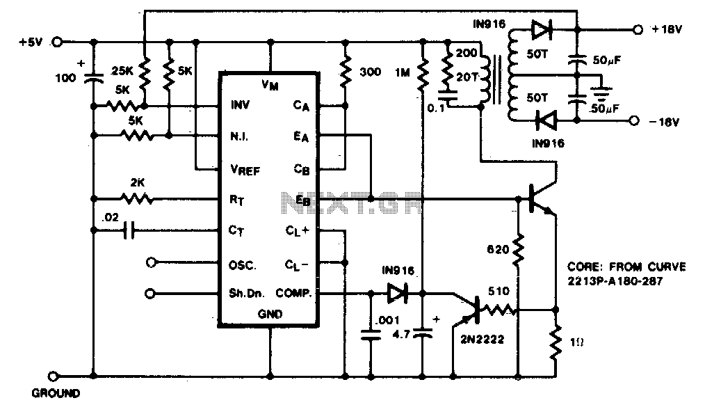
A low-current flyback converter is utilized to generate ±15 volts at 20 mA from a +5 volt regulated line. The reference generator in the SG1524 is not used, with the input voltage serving as the reference. Current limiting in...
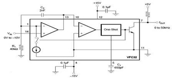
The circuit diagram of a voltage-to-frequency (V/F) converter is presented, designed to handle negative input voltage. It employs the VFC32 voltage-to-frequency converter, which is commonly utilized in various applications. The V/F converter circuit is essential in converting an analog voltage...
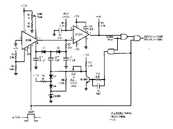
The simple 4-digit converter circuit has an output count of 1, designed to operate within a frequency range of f-IMHz to 10.000. All diodes used in the circuit are IN4146, and the capacitors are made of `POLYSTYRENE` NPO. The...
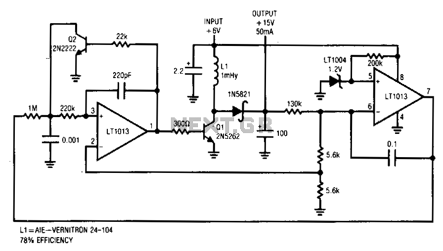
This converter delivers up to 50 mA from a 6-V battery with 78% efficiency. This flyback converter functions by feedback-controlling the frequency of inductive flyback events. The inductor's output is rectified and filtered to de-bias the feedback loop to...

This is a DC to DC converter circuit designed to take an input of 12V to 24V at 4A and convert it to an output of 24V to 48V at 2A. The circuit utilizes simple components, including a CMOS...
The circuit accepts two positive voltage inputs, VN and Vv, and provides a TTL-compatible output pulse train whose repetition rate is proportional to the ratio VN/V0. The full-scale output frequency is approximately 100 Hz, and the linearity error is...