
PERIOD TO VOLTAGE CONVERTER

The described circuit operates on the principle of pulse generation and signal conditioning. Upon receiving a low-to-high transition at the input, a narrow positive pulse is produced at point A. This pulse triggers a voltage drop to -13 V at point B, effectively disabling diode D2, which is crucial for preventing reverse current flow in the circuit. As a result, the V+ terminal of the integrated circuit ICC is brought down to zero, indicating that the circuit is in a quiescent state with no active voltage supply.
The charge present on capacitor C1 is rapidly absorbed by the ICC, ensuring that the circuit can quickly respond to subsequent input changes. The discharge time of capacitor C2, in conjunction with resistor R5, is determined by their time constant, which is approximately 10 picoseconds. This rapid discharge is essential in high-speed applications where timing and signal integrity are critical.
The buffer ICB is designed to provide isolation between stages while maintaining signal integrity. Its gain is calculated using the resistors R8 and R9, following the formula provided. This gain allows for appropriate amplification of the signal while ensuring that the output remains stable and within desired parameters.
The average voltage at ICD is derived from the specified formula, indicating the relationship between the input signal and the output voltage, which is critical for ensuring that subsequent stages in the circuit receive the correct signal levels.
Finally, the combination of resistor R10 and capacitor C3 serves to smooth the sawtooth waveform generated in the circuit, converting it into a stable DC output. This smoothing process is vital for applications where a clean DC signal is required for further processing or utilization in other parts of the system. The careful selection of component values for R10 and C3 will dictate the effectiveness of the smoothing action and the quality of the output signal.When the input goes from low to high, a narrow positive pulse is generated at point A. This pulse becomes - 13 V at point B, which cuts off D2. ICC`s V+ voltage becomes zero. The charge on C1 will be absorbed by ICC on in a short time. The time constant of C2 and R5 determines the discharge period-about 10 ps. ICB is a buffer whose gain is equal t o (R8+R9)G·R9-1. 545. ICD`s average votiage will be (1362fx1. 545)G·2=1052t. R10 and C3 smooth the sawtooth waveform to a dc output. 🔗 External reference
Related Circuits
This DIY 12V to 220V DC to AC converter utilizes a CMOS 4047 as its main component, effectively transforming 12V DC into 220V AC. The circuit design of this DC to AC converter primarily revolves around the CMOS 4047 integrated...
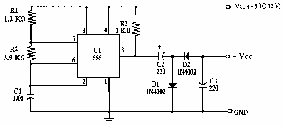
This circuit inverts the polarity of the input. Output is limited to less than 200mA. More: U1 NE555 timer IC R1 1.2k ohm resistor R2 3.9k ohm resistor R3 1k ohm resistor C1 0.05 uF ceramic capacitor C2, C3...
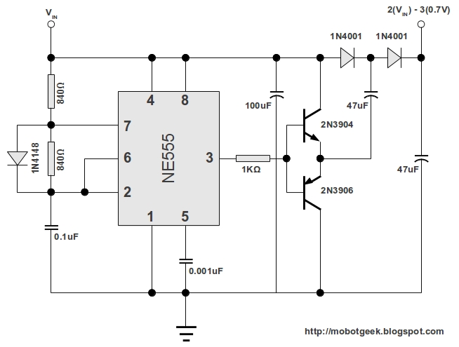
This DC voltage doubler circuit generates a voltage that is double its supply voltage. It is advantageous when a higher voltage level is required from a single lower voltage power supply. Due to the low current consumption in such...
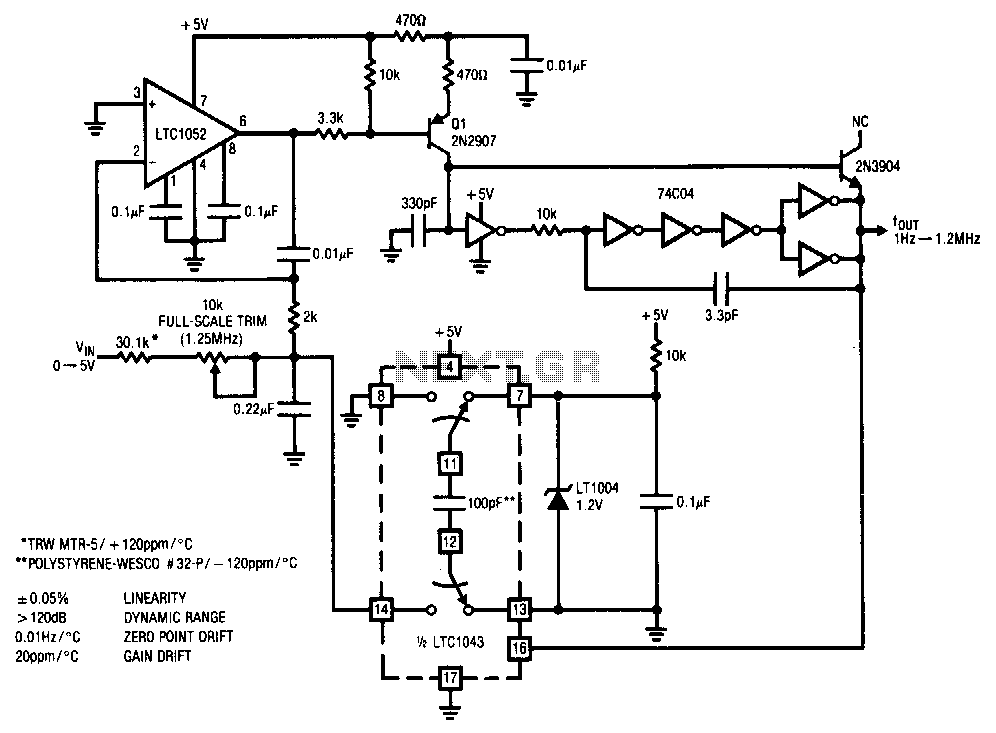
This stabilized voltage-to-frequency converter operates within a range of 1 Hz to 1.25 MHz, featuring a linearity of 0.05% and a typical temperature coefficient of 20 ppm/°C. The circuit is powered by a single 5-V supply. It employs a...
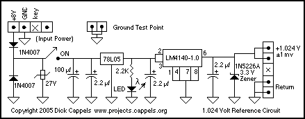
A keyed power input connector, series rectifier and a shunt rectifier, both 1N4007, prevent reverse voltage from being applied to the power input. A 27 volt metal oxide varistor clamps the voltage to the 78L05 that follow it, to...
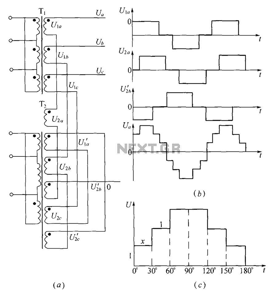
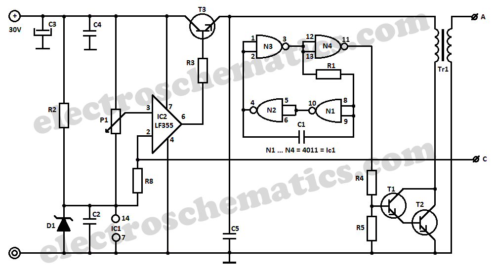
As shown, (a) for the three-phase step wave inverter output transformer winding connections; (b) in the figure, its output waveform. The three-phase step wave inverter is designed to convert direct current (DC) into a three-phase alternating current (AC) output. This...