
Pierce oscillator

The circuit described features an oscillator configuration utilizing a transistor (Q1) in conjunction with a crystal for frequency stabilization. The crystal is strategically positioned between the collector and base of Q1, which facilitates the generation of oscillations at a precise frequency determined by the characteristics of the crystal. This setup is typical in oscillator circuits where stability and accuracy are paramount.
To enhance feedback within the circuit, a capacitor (C2) is connected across the collector-emitter junction of Q1. This capacitor plays a critical role in shaping the feedback loop, ensuring that the oscillations are sustained and stable. The inclusion of C2 allows for better control over the phase shift and gain, contributing to improved performance of the oscillator.
Additionally, transistor Q2 serves as an output buffer. This component is essential for isolating the oscillator stage from subsequent circuitry, thereby preventing loading effects that could dampen the oscillations. The output buffer allows for a stronger drive capability, enabling the oscillator to interface effectively with other components or stages of the circuit without compromising the integrity of the oscillation signal.
Overall, this configuration exemplifies a common approach in electronic oscillator design, where stability, feedback control, and output buffering are critical considerations for successful operation.The oscillator transistor is Ql, and the crystal is placed between the collector and base. Feedback is improved by the use of the collector-emitter capacitor C2 Transistor Q2 is used as an output buffer.
Related Circuits
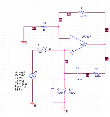
In this laboratory experiment, the objective is to design the frequency-determining network for a 1 kHz sinusoidal oscillator. The specified values are as follows: Capacitance = 100 nF and Resistance = 1520 ohms. The output voltage waveform of the...
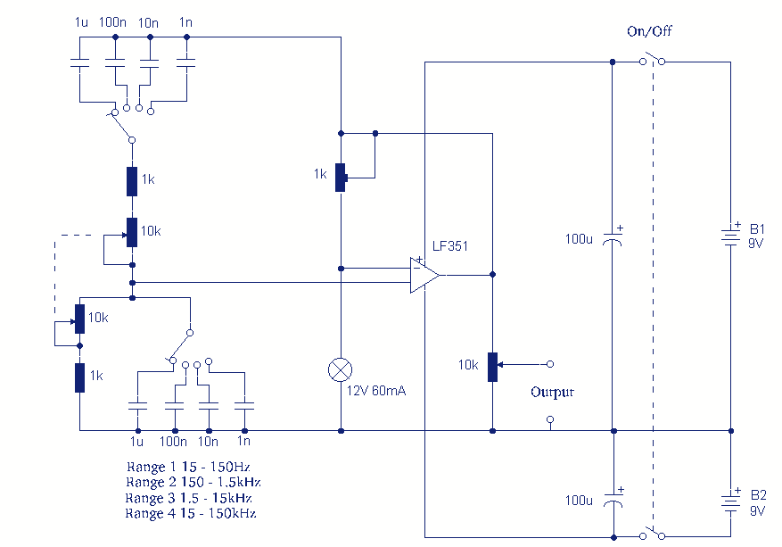
In this circuit the gain is provided by a FET type op-amp. I have used an LF351, which may be hard to obtain, but the TL071CN or TL081CN may be used and have a faster slewing rate than the...
The following file contains detailed information about the design of a basic clock oscillator circuit diagram. Included in this file is information about selecting the components. The clock oscillator circuit is a fundamental component in various electronic systems, providing a...
The 555 Timer IC operates in three modes: monostable, astable, and bistable/Schmitt trigger. This article will focus on its astable mode. The astable mode of the 555 Timer IC is characterized by its ability to generate a continuous square wave...
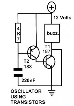
This schematic diagram represents a basic oscillator circuit utilizing two transistors. When the transistors and several passive components are connected as illustrated, the circuit begins to oscillate. The oscillation frequency can be modified by altering the values of either...
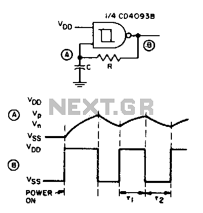
Before power is applied, the input and output are at ground potential, and capacitor C is discharged. Upon power-on, the output transitions to high (Vdd), and capacitor C charges through resistor R until a specified voltage (V) is reached;...