
PLL FM Demodulator Circuit Module

The circuit functions effectively by utilizing the CD4046B integrated circuit, which incorporates both a VCO and phase comparators. The VCO generates a frequency that is controlled by the input voltage, allowing it to lock onto the frequency of the incoming FM signal. The phase comparator compares the phase of the VCO output with the phase of the incoming FM signal to maintain synchronization.
In this setup, the AC coupling at the input stage is crucial for filtering out any DC offset present in the incoming signal, ensuring that only the varying part of the signal is processed. This is particularly important in FM demodulation, where the information is encoded in the frequency variations of the carrier wave.
The choice of Phase Comparator I is significant as it offers better performance in terms of noise rejection, which is essential in demodulating FM signals where the signal-to-noise ratio can be critical. The PLL's ability to maintain a stable output frequency that corresponds to the modulated audio signal makes it highly effective for applications in radio communications and audio processing.
Overall, this PLL-based FM demodulator circuit provides a reliable means of extracting audio information from frequency-modulated signals, making it suitable for various electronic communication systems. The design ensures that the demodulated output is a faithful reproduction of the original audio signal, which is critical for clarity and quality in audio applications.This is a circuit about PLL system that can be used to implement an FM demodulator. Since the VCO output tracks the FM signal, and the VCO input voltage is proportional to the VCO output frequency, then the VCO input will be equal to the demodulated signal. This circuit is based on phase comparator and VCO. This is the figure of the circuit. For t his example, an FM signal consisting of a 10-kHz carrier frequency was modulated by a 400-Hz audio signal. The schematic diagram shows the connections of the CD4046B as an FM demodulator. The total FM signal amplitude is 500 mV, therefore, the signal must be ac coupled to the signal input (terminal 14).
Phase comparator I is used for this application because a PLL system with a center frequency equal to the FM carrier frequency is needed. Phase comparator I lends itself to this application also because of its high signal-input-noise-rejection characteristics.
🔗 External reference
Related Circuits
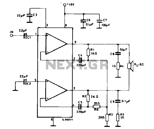
The schematic illustrates a 12 W Bridge Amplifier circuit diagram utilizing the TDA2007A, a class AB dual audio power amplifier. This amplifier is specifically designed for stereo applications in music centers, television receivers, and portable radios. As stated in...

If you need a timer circuit, we go after the most proven 555. However, if the delays are longer, based on timing capacitor capacity is too large. In this case, a circuit of Figure 1 After pressing the button...
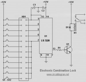
This circuit diagram represents a simple electronic combination lock utilizing the IC LS7220. The circuit is designed to activate a relay for controlling any device (on and off) each time a specific combination of four digits is entered. It...
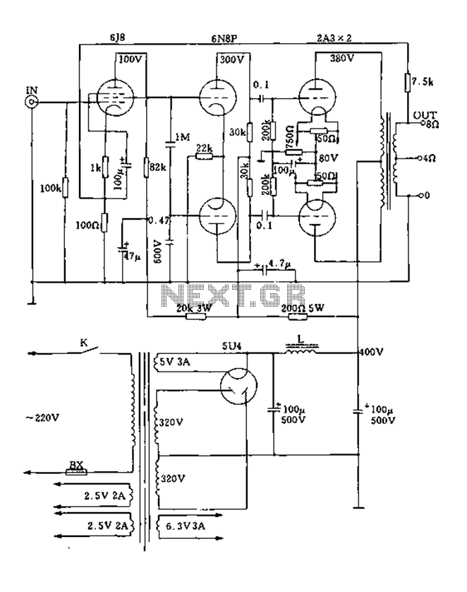
FIG. 2A3A is a low direct thermal resistance transistor with a resistance of only 800 ohms. The output transformer has a primary screen to load impedance of 3.5k ohms. The push-pull amplifier tube operates with a screen voltage ranging...
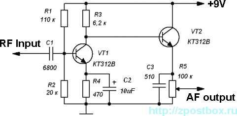
This is a highly sensitive envelope detector designed for AM radio applications. The circuit, illustrated in Figure 1, enables linear detection of weak signals with a modulation depth of 80-85%. The first stage (VT1) functions as a common-emitter amplifier...
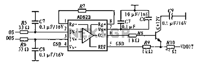
The AD623 is an integrated 3-way amplifier that can operate with either a single or dual supply. It features high common-mode rejection ratio (CMRR) and low voltage drift, along with programmable gain control via an external resistor. All components...