
power amplifier class circuit

The Class A power amplifier schematic is designed to provide high-fidelity audio amplification, making it suitable for high-end audio applications. The continuous current flow in the output devices minimizes crossover distortion, a common issue in Class B amplifiers. The use of a quasi output stage allows for a simpler design while maintaining low distortion characteristics.
In this circuit, the negative feedback loop plays a crucial role in maintaining stability and linearity across the amplifier's operating range. The 30dB NFB factor at 20 kHz implies that the amplifier is capable of maintaining a consistent gain while effectively reducing distortion and improving frequency response. The feedback network is likely composed of resistors and capacitors that tailor the frequency response to ensure that the amplifier performs well across the audio spectrum.
The choice of a CFP stage as an alternative to the quasi output stage can further enhance performance. The CFP configuration provides better thermal stability and allows for higher current gain, which can be beneficial in driving low-impedance loads without compromising sound quality.
The implementation of the LM385 reference voltage regulator ensures that the biasing of the output stage remains stable, which is essential for consistent performance. The voltage divider that reduces the reference voltage is critical in setting the appropriate bias current for the output devices, allowing them to operate in the desired Class A mode.
Overall, this Class A power amplifier design exemplifies a balance between performance and complexity, making it a suitable choice for audiophiles seeking high-quality sound reproduction. The attention to detail in the circuit design, particularly in the output stage and feedback mechanism, contributes to its ability to deliver clear, distortion-free audio signals.This is a design schematic Class A power amplifier. This is a close as possible in operating parameter the Under Classes is class B, to aid comparison ; in particular the NFB factor remains 30dB at 20 kHz. The front end is similiar to class B amplifier. This circuit uses a standart quasi output. This may be replaced by a CFP stage without proble ms. In both cases the distortion is extremely low, but gratifyingly the CFP proves even better than quasi, confirming the simulation results for output stages in isolation. About Class-A amplifier, in this class is the highest class from another class. Classes below begin from AB to Class S. In a Class-A amplifi er current fl ows continuously in all the output devices, which enables the nonlinearities of turning them on and off to be avoided.
They come in two rather different kinds, although this is rarely explicitly stated, which work in very different ways. The fi rst kind is simply a Class-B stage (i. e. two emitter-followers working back to back) with the bias voltage increased so that suffi cient current fl ows for neither device to cut off under normal loading.
The great advantage of this approach is that it cannot abruptly run out of output current; if the load impedance becomes lower than specifi ed then the amplifi er simply takes brief excursions into Class-AB, hopefully with a modest increase in distortion and no seriously audible distress. The operation of current regulator TR13, TR15, TR 16 has already been described. The reference used is a National LM385/1. 2 Its output voltage is fixed at 1. 233 V nominal ; this is reduced approximately 0. 6V by 1k - 1k divider. The circuit is the best for me, because is loudly, and does not vibrate the speakers leaves, softly sound, and low noise.
And i like it. , . , :) 🔗 External reference
Related Circuits
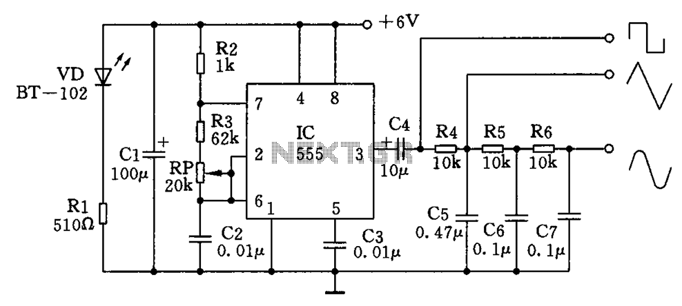
The circuit simultaneously generates a square wave, triangle wave, and sine wave, making it particularly suitable for electronics enthusiasts and students who wish to observe signal waveforms using an oscilloscope. This signal generator circuit is simple, low-cost, and allows...
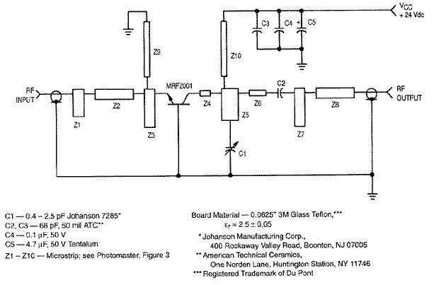
RF amplifier circuit diagram, delivering 1W for 2.3GHz, built based on MRF2001. This RF amplifier provides approximately 1 Watt power output with a minimum gain of 8 dB at a 24V voltage supply. The frequency can be tuned from...
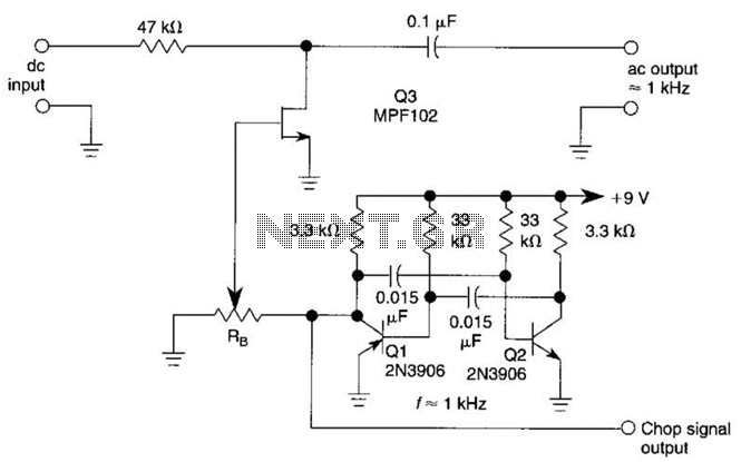
A JFET (MPF102) is utilized to chop a DC signal for amplification in an AC-coupled amplifier. Q3 serves as the chopper element, while Q1 and Q2 create a multivibrator to generate the chopping signal. Additionally, resistor Rr establishes the...
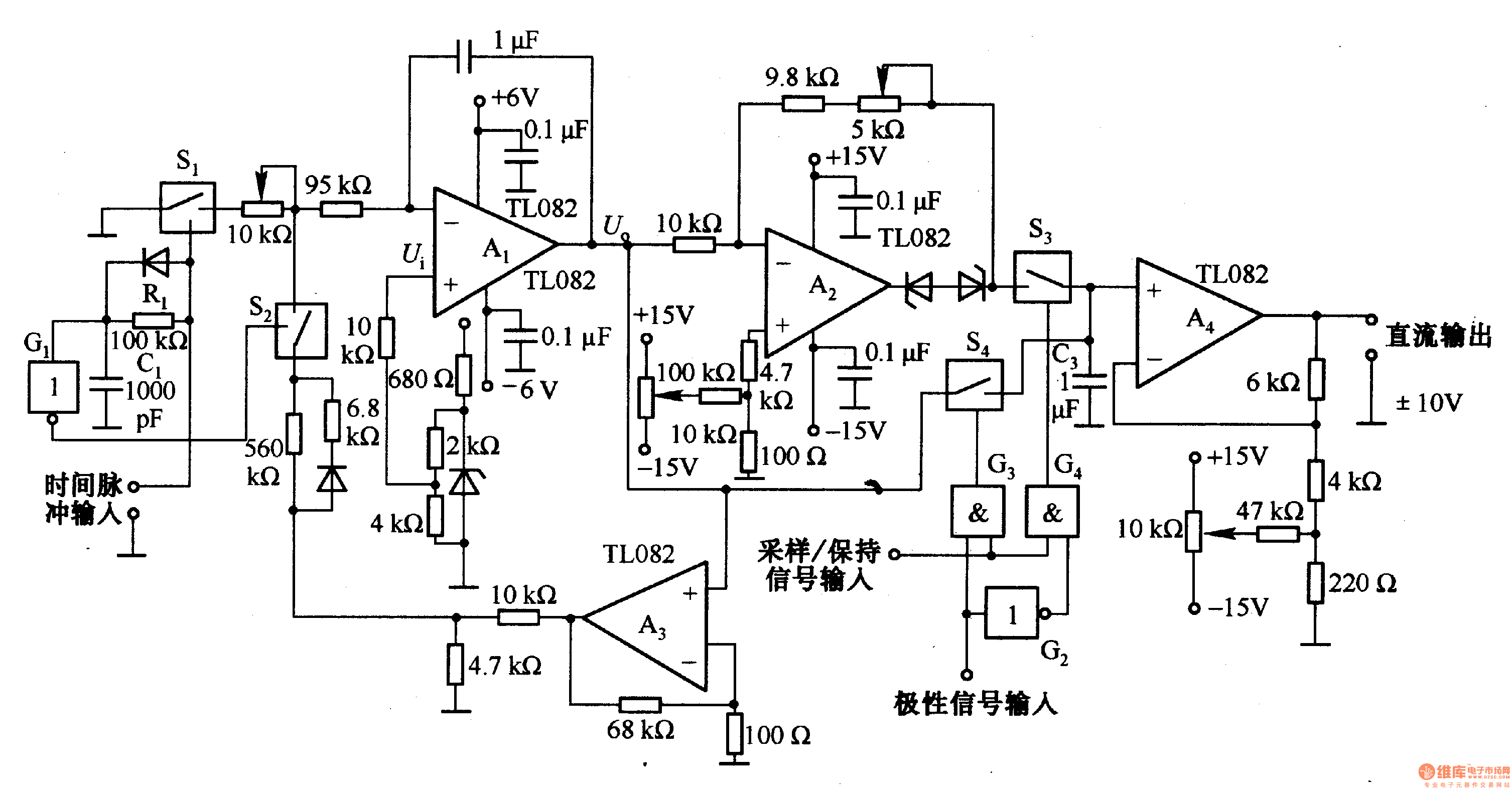
This circuit is designed for pulse width (time) to voltage conversion. According to the component parameters in the diagram, it can convert a pulse width of 0.1 seconds into an output voltage of 10V. When a conversion pulse is...
The CD4013 is a dual D flip-flop that operates on the rising edge of the clock signal. Its internal block diagram and pin configuration are provided. This device is part of the standard model C043 and the GB model...

Cascaded amplifier sections are utilized to extend bandwidth and increase gain. By employing two HA-2539 devices, this circuit achieves a gain of 60 dB at 20 MHz. The design of the cascaded amplifier circuit involves connecting multiple amplifier stages in...