
Power amplifier for Loudspeaker 6.5W 8R circuit

The described amplifier circuit employs a negative feedback mechanism to stabilize the load current, making it less sensitive to variations in the loudspeaker's impedance. This is particularly advantageous in audio applications where consistent performance is desired. The feedback loop is established through the voltage generated across R7, which directly influences the inverting input of operational amplifier IC1.
The gain formula, (Zo + R7) / R7, indicates that the circuit is designed to provide a substantial amplification factor, which is critical for driving low-impedance loads like loudspeakers. The choice of R7 is vital in setting the gain, and a careful selection of this resistor can optimize performance based on the specific loudspeaker characteristics.
The unconventional grounding of IC1's output allows the circuit to draw base current for the output transistors from the power supply rather than from the operational amplifier. This design choice enhances the amplifier's robustness, as it reduces the load on IC1, allowing it to focus on signal processing rather than power delivery.
The quiescent current, set by R2, R3, R5, and R6, plays a crucial role in defining the amplifier's operating class. In Class A operation, maintaining a quiescent current of 50 mA to 100 mA ensures linear amplification with minimal crossover distortion. Matching transistors Q1 and Q2 is essential to maintain balance in the output stage, preventing significant deviations in current and voltage that could lead to distortion.
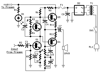
The output stage is designed to handle a substantial emitter current of approximately 500 mA under full load conditions, which is suitable for driving an 8-ohm loudspeaker effectively. The low total harmonic distortion (THD) of 0.01% at the specified output power indicates high fidelity in audio reproduction, making this amplifier circuit suitable for high-quality audio applications. Overall, this design exemplifies careful consideration of feedback mechanisms, component selection, and biasing strategies to achieve optimal performance in audio amplification.The amplifier of circuit, use negative current feedback. So, the load current depends mainly from the input signal and no so much from the impedance of loudspeaker. The inductor current of loudspeaker develop above in the R7 a voltage. This voltage is drive to the inverting input of IC1, creating thus negative feedback. Total voltage gain of circu it, it depend from the reason of impedance of loudspeaker H1 [ Zo ], to the price of R7. In the circuit the gain is (Zo+R7)/R7 that is to say (8+0. 5)/0. 5=17. The connection output of IC1 in the ground, is extraordinary, but in this way, the current of base of transistors Q1, Q2 is provided by the lines of supply and no by the IC1. The calm current of is 50 until 100mA, for operation in Class A and is determined by R2, R3, R5, R6. Transistors Q1-Q2, should be matching, so that are not created big current and voltage of deviation. May it will are change the resistors R2, R3, so that we achieve symmetry of bias. With complete drive, the current of emitter the Q1-Q2 is roughly 500mA. The THD is 0. 01% for output power, 6. 5W in 8R and voltage supply ± 18V. Elektor`87 🔗 External reference
Related Circuits
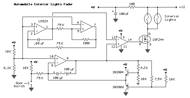
The circuit utilizes the LM324 low-power operational amplifier, which consumes approximately 3mA of current. This low current draw ensures that the battery will not be adversely affected if the circuit remains connected for extended durations. The LM324 is a quad...
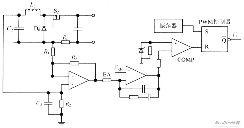
The circuit is capable of enhancing the system power factor to a value exceeding 0.99. It effectively reduces the waveform distortion of the input supply current, ensuring compliance with GB15144 standards, with a distortion index lower than level L....
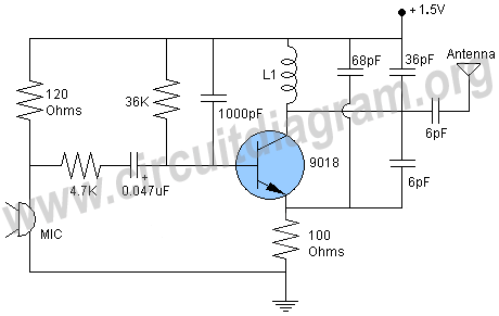
A simple whole house FM transmitter circuit diagram and description. Operating power is a 1.5V battery of any type. This circuit is able to transmit at a distance of 30 meters. The whole house FM transmitter circuit operates on a...
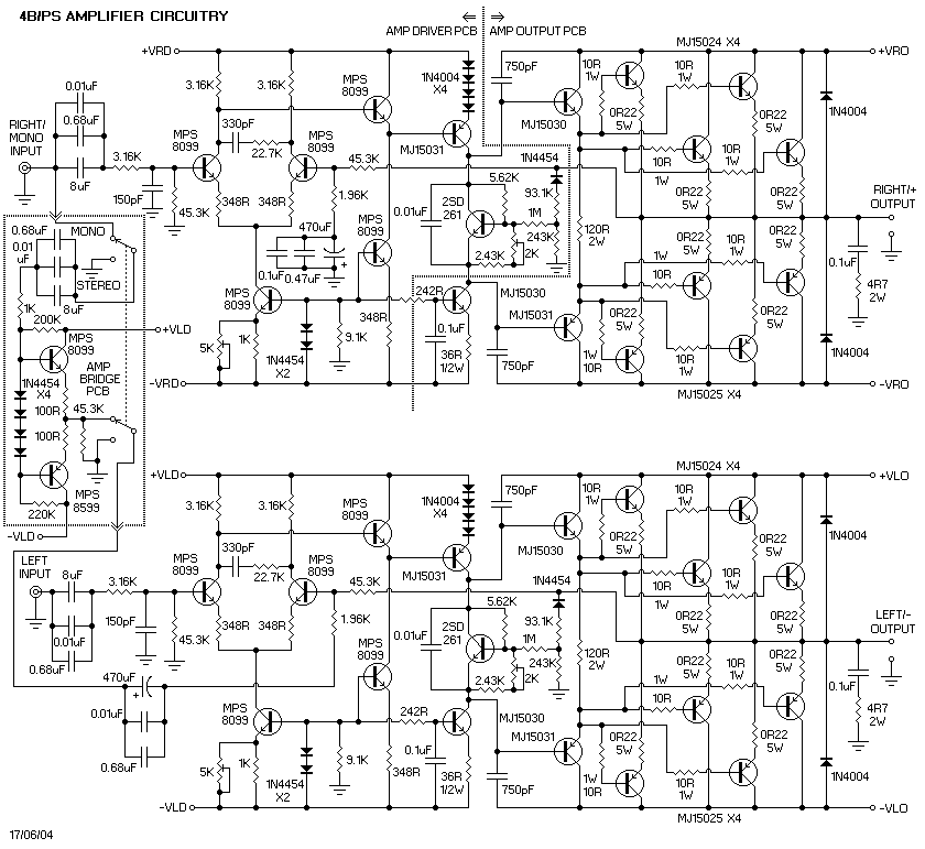
It is important to note that there is limited protection circuitry and fuses in this amplifier. A short turn-on delay for the output power supply is included to minimize thumps, along with a couple of line fuses, but no...
This is a 3U rack unit with standard mains power supply. It provides audio routing and speed control for two domestic three-head cassette tape machines such that they can be used to create authentic 1960s style tape flanging effects....
60W Bass Amplifier. It features low-cut and bass controls. The output power is 40W on 8 Ohm loads and 60W on 4 Ohm loads. An amplifier circuit diagram is provided. The 60W bass amplifier is designed to deliver robust audio...