
Precision Amplifiers

To analyze the situation, it is essential to understand the configuration and functionality of the operational amplifiers involved. The op amp in question, when tested in a buffer configuration, should ideally provide a straightforward output that reflects the input voltage, confirming whether the device is operational. If the output deviates significantly from the expected behavior, it may indicate a fault within the op amp itself.
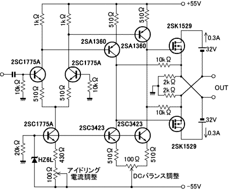
The voltage discrepancies noted at V_SONIC_RX_BIAS2, pin 7, and V_SONIC_RX suggest that there may be issues with the biasing or potential dividers within the circuit. The difference in voltage levels between op amp A and op amp B could be indicative of varying load conditions or feedback configurations affecting their performance. The non-inverting configuration of the op amps should produce specific gain characteristics, and any deviation in output suggests that further investigation into the circuit layout, component values, and connections is warranted.
Furthermore, it is advisable to perform a thorough examination of the surrounding circuitry, including any resistors, capacitors, or other components that may influence the operation of the op amps. By isolating each stage of the circuit and confirming the integrity of each component, a clearer understanding of the root cause of the discrepancies can be achieved, leading to a more effective troubleshooting process.Also you have mentioned that the op amp in the second stage gets damaged. Can you confirm that by testing that op amp in a buffer configuration(or any simple configuration) I am asking you to do this because we need to know if the part is actually failing or is it something else in the circuitry which is causing it to behave like this. I see. But why the potential at V_SONIC_RX_BIAS2 is 1. 8V and at pin 7 is 2. 5V while the V_SONIC_RX is 3. 0V and why is this different from the op amp-A (1. 5V on bias voltage and pin 3 of op amp-A). u also see the photos in my previous emails when the op amp is in non-inverting configuration. op amp A vs op amp B. the output of op amp B is different from output of op amp A. 🔗 External reference
Related Circuits
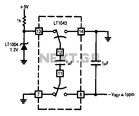
This circuit enables the inversion of a reference signal with an accuracy of 1 ppm. It features high input impedance and does not require any trimming. The described circuit is designed to invert a reference voltage signal while maintaining a...
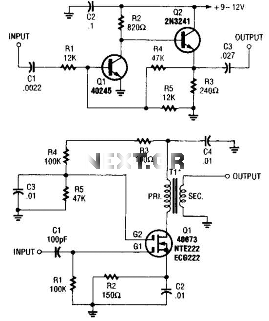
These two buffer/amplifiers have been effectively utilized with variable frequency oscillators (VFOs): one (depicted in A) is constructed using a pair of bipolar NPN transistors, while the other (illustrated in B) is designed around a dual-gate MOSFET. The first buffer/amplifier,...
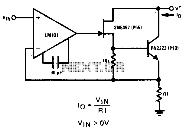
The 2N5457 JFET and PN2222 bipolar transistor exhibit high output impedance. Employing Rl as a current sensing resistor to feedback into the LM101 operational amplifier yields significant loop gain for negative feedback, thereby improving the circuit's capability as a...
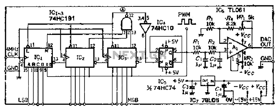
A PWM clock signal is generated at 4096 times the input frequency, counting up (Q3) until the base of ICi-IC3 is full. The output point produces a maximum clock signal. On one side, voltage data is loaded into IC3,...
The amplifier in question is comparable to another model that has a lower parts count. It is worthy of construction. The amplifier under discussion features a simplified design that maintains high performance while reducing the number of components required for...
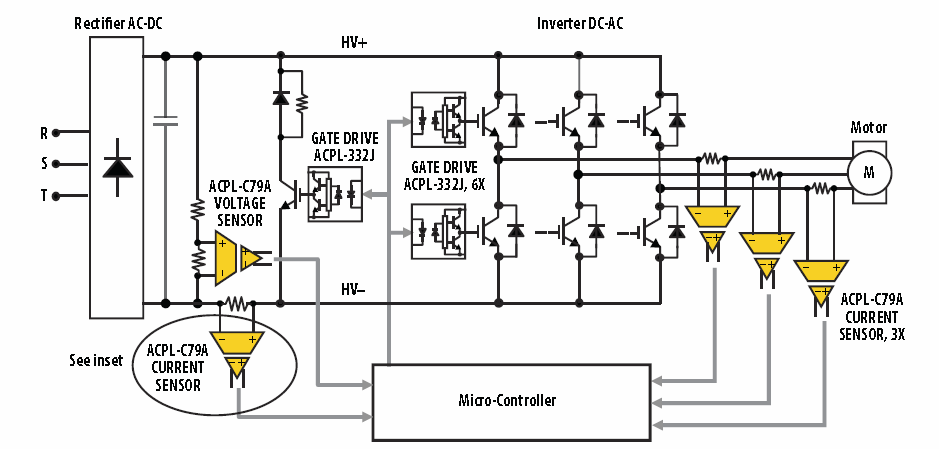
Insulated-gate bipolar transistors (IGBTs) require comprehensive protection to prevent damage and failures due to conditions such as short circuits, overloads, and overvoltages. This protection is essential for ensuring safe and stable operation of power converters in applications including motor...