
Precision-Increasing Buffer

In an analog circuit, the integration of a unity-gain buffer is a strategic enhancement that significantly improves signal integrity and precision. The operational amplifier IC1, characterized by its maximum offset voltage drift of 1.8 µV/°C, is capable of driving a load of 600 ohms. The power dissipation of IC1 under these load conditions is calculated to be 94 mW, which is critical for thermal management in circuit design. The thermal resistance (θJA) of 150°C/W indicates that for every watt of power dissipated, the junction temperature will rise by 150°C. This results in a change in output voltage of 25 µV, which could adversely affect the precision of the circuit.
By incorporating a unity-gain buffer IC2, the design effectively isolates IC1 from the load, thus preventing variations in power dissipation from affecting the operational characteristics of IC1. This isolation is crucial for maintaining the minimum rated offset voltage, ensuring that the output remains stable and accurate. The loop gain of IC1 plays a vital role in this configuration, as it serves to cancel out any potential offset introduced by the buffer, thereby preserving the integrity of the signal.
When selecting a suitable unity-gain buffer, it is essential to consider its bandwidth characteristics. A buffer with a 3-dB bandwidth at least five times greater than the gain-bandwidth product of the operational amplifier will ensure that the buffer operates effectively within the desired frequency range without introducing significant phase shifts or distortion. This consideration is paramount for applications requiring high precision and reliability in analog signal processing. Adding an unity-gain buffer to your analog circuit can increase its precision. For example, by itself, the op a mp IC1 exhibits a maximum dVosldT of 1.8 /iV7°C and can drive a 600- load. Under these conditions, IC1 would dissipate 94 mW incrementally. Thus, the op amp"s 0JA of 150°C/PFr would change its vqs by 25 juY. The buffer, IC2, will isolate IC1 from the load and eliminate the change in power dissipation in IC1, thereby achieving ICl"s minimum, rated offset-voltage drive. The loop gain of IC1 essentially eliminates the offset of the buffer. Almost any unity-gain buffer will work, provided that it exhibits a 3-dB bandwidth that is at least 5 times the gain-bandwidth product of the op amp.
Related Circuits
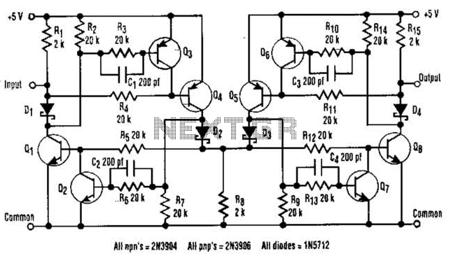
The I2C serial bus is a widely used two-wire bus for small-area networks. The I2C Clock and Data lines feature open collector (or drain) outputs for each device on the network, requiring only a single pull-up resistor. This architecture...
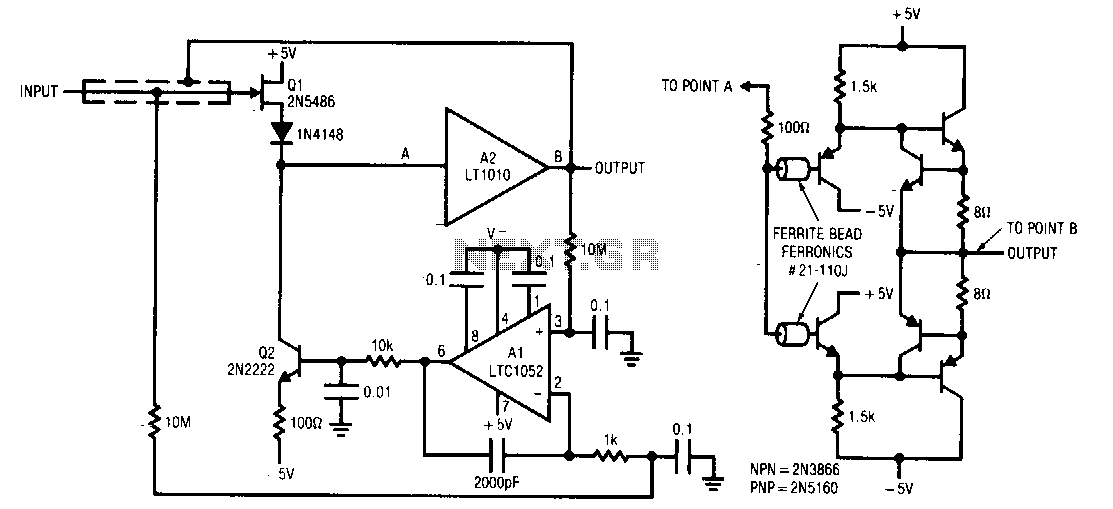
Q1 and Q2 form a simple, high-speed FET input buffer. Q1 operates as a source follower, while Q2 serves as a current-source load that regulates the drain-source channel current. The LT1010 buffer is utilized to provide output drive capability...
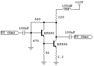
A 3KHz-50MHz signal generator is available, and there is a requirement to amplify its 2.3mW output to +7dBm. The need is for a broadband amplifier capable of achieving this amplification. To amplify the output of a signal generator from 2.3mW...
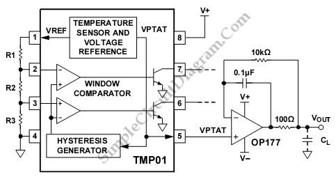
This is a buffer circuit for the TMP01 temperature sensor. The output of this sensor is a low impedance DC output voltage with a 5 mV/K temperature coefficient. The buffer circuit designed for the TMP01 temperature sensor serves to isolate...
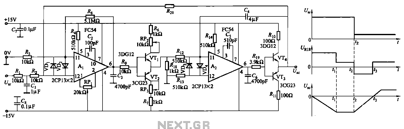
The ZKJ-S-type buffer controller circuit is designed for motor starting slip control. This buffer controller is composed of two operational amplifiers, Ai and Az. The operational amplifier Ai functions as a speed amplifier that saturates, while Az acts as...
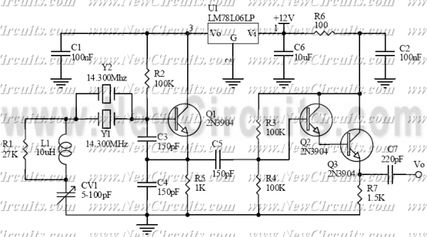
The circuit is a VXO with buffered output. It operates on the 20-meter amateur radio band with the output voltage about 0.2 Vp-p. The crystal frequency is pulled by tuning the variable capacitor CV1 about 36 kHz with only...