
precision phase locked loop circuit

The precision Phase Locked Loop (PLL) circuit is designed to maintain a stable output frequency that is synchronized with a reference input frequency. This circuit utilizes a phase detector, a low-pass filter, and a voltage-controlled oscillator (VCO) to achieve its functionality. The enhancements implemented in this PLL include the incorporation of flip-flops with a clearing mechanism, which significantly improves the response time of the phase detector.
In this configuration, the phase detector compares the phase of the input signal with the output signal from the VCO. The output of the phase detector is a pulse-width modulated signal that represents the phase difference between the two signals. The presence of gate G1 allows for the immediate clearing of the flip-flops, ensuring that the phase detection process can quickly adapt to changes in the input signal.
The integration of currents by operational amplifier A1 is crucial for the PLL's performance. The steering of these currents through transistors Q1, Q2, Q3, and Q4 is strategically implemented to enhance the speed of the circuit. Transistors are selected for this purpose due to their rapid switching capabilities, which help in reducing latency in the phase comparison process.
The output from the low-pass filter, which processes the pulse-width modulation signal, is fed into the VCO. The VCO generates a frequency that is adjusted based on the filtered output, effectively locking onto the reference frequency. This feedback loop continues to operate, maintaining synchronization between the output frequency and the reference input frequency, even in the presence of varying load conditions or input signal variations.
In summary, the precision PLL circuit described is an advanced implementation that leverages the speed of transistors and the efficiency of flip-flops to achieve a highly responsive and stable frequency synchronization system. The design elements, such as the clearing gate and current steering through transistors, contribute to the overall performance and reliability of the PLL in various applications.The precision Phase Locked Loop PLL in this circuit acts very much the same as the basic PLL, with refinements in various places. The flip-flops in the detector have a gate G1 to CLEAR them, for quicker response. The currents which A1 integrates are steered through Q1, Q2 and Q3, Q4 because transistors are quicker..
🔗 External reference
Related Circuits
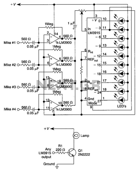
This circuit will produce an output when the sound exceeds a preset level. The LM3915 is a log-output bar graph driver. A transistor driver is used for higher current loads. To drive heavy-current loads with an LM3915 output, a...
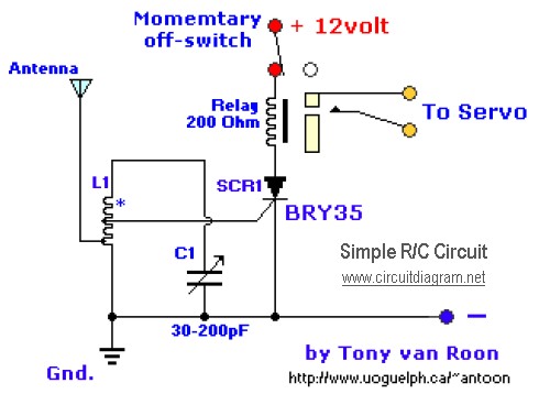
The diagram illustrates a straightforward and efficient receiver designed for activating garage doors, starter motors, alarms, warning systems, and various other applications. The silicon-controlled rectifier (SCR) utilized in this circuit features an exceptionally low trigger current of 30 µA,...
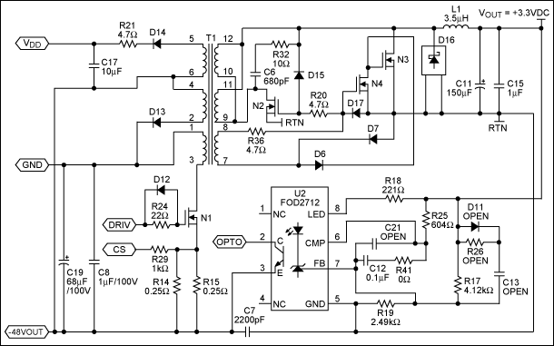
A PoE Plus power level of 30 W can be achieved by utilizing an external MOSFET along with a controller that is compatible with the older standard. Power over Ethernet (PoE) technology enables the delivery of electrical power along with...
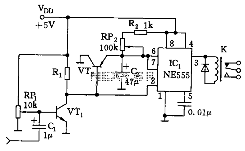
The timing circuit utilizes the 556 dual time base circuit, which includes an intermediate access N8281 crossover network. This design does not require a large volume capacitor, allowing for extended time delays. Initially, the first half of the 556...
The 2.25-MHz oscillator Q1 drives amplifier Q2 and XTAL1, an ultrasonic transducer. The transducer is a lead zirconate-titanate type. Taps on T1 and T2 provide low-impedance drive points. The circuit consists of a 2.25-MHz oscillator (Q1) that serves as the...
A sensitive and reliable RF field strength meter is an invaluable instrument in amateur radio and in the radio-controlled model area. A field strength meter is. A radio frequency (RF) field strength meter is a specialized device used to measure...