
Precision QRP Transmitter

If you build this transmitter, MAKE SURE that the oscillator you use is a TCXO, not just a packaged oscillator. Many old computer cards include such oscillators, and some will be on 14. 31818MHz - very tempting, but don`t be fooled - they are not stable enough. The output of the TCXO is typically AC coupled, and a clipped sinewave about 1V p-p. This is insufficient to drive CMOS directly, but if biassed to half-supply by two 100k resistors, will reliably clock the first 74HC74 divider, U1A.
This D flip-flop is arranged to divide by two through the expedient of connecting the /Q inverting output to the D input. If you are lucky enough to locate a TCXO with CMOS output, just omit the two resistors. The second flip-flop, U1B, is also arranged to divide by two. In this case the /CLR (reset) input (pin 13) is held high by a resistor, and when power is applied, the capacitor on this pin holds the divider in reset (Q output low) until after the TCXO has reliably started.
The 10nF capacitor charges to 5V through the 100k resistor to remove reset after about 1ms. Without this addition, the divider might randomly start with the output high, and since the TCXO may take up to several hundred µs to start, the PA stage could be turned hard on and draw excessive current. If necessary, the transmitter may be turned on and off by connecting a switch from this point (U1B pin 13) to ground.
Keying the transmitter for ID purposes at this point may however lead to strong key clicks, and the logic is inverted from that of a normal key (which keys to ground to transmit). Power for the CMOS device and the TCXO is derived from a simple shunt regulator. Zener diode D1 holds the voltage at about 4. 7V, using current from the 12V supply via the 470 © resistor. If you wish, you could use two red LEDs and a 1N4002 in series in place of the Zener diode to achieve about 4.
7V, and have a front panel LED power indicator at no extra current drain. The shunt regulator, TCXO and divider draw about 15 to 20mA in total. Most of the current goes into driving the PA gate circuit. The PA stage draws about 80mA for an input power of about 900mW. The PA stage is shown at the right (power FET Q1), and is gate driven with a 50% duty cycle waveform. Capacitive coupling ensures that the transistor turns off if drive is inadvertently lost, as always happens briefly at switch-on.
The resistor to ground ensures that the transistor stays off without drive. The diode D2 is a clamp which ensures that the drive is all positive, 0 - 4V, rather than -2V to +2V. This type of FET has a switch-on voltage of about 2. 5V, and can be adequately driven by a single CMOS gate. Don`t use bigger FETs as the gate capacitance will be too large for the CMOS driver to handle. If smaller FETs (such as 2N7000) are contemplated, use several parallel devices to achieve sufficiently low on resistance - otherwise the FET will get rather hot.
The chosen FET is a small surface-mount N-channel power 🔗 External reference
Related Circuits

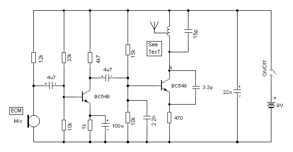
The modification presented involves using a 2N2219 NPN transistor to replace T2 and a 2N3553 NPN transistor to replace T3. Both transistors are categorized as VHF transistors. It is necessary to attach a heatsink to the last transistor. No...
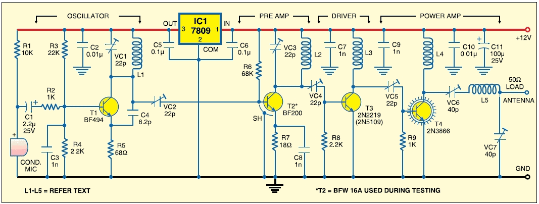
The circuit was designed to operate a frequency modulation voice transmitter over the FM band within the VHF frequency range. The transmitter is an electronic device. The frequency modulation (FM) voice transmitter circuit operates within the VHF (Very High Frequency)...
This is a highly stable, harmonic-free, long-range FM transmitter circuit designed for FM frequencies between 88 and 108 MHz. It is capable of covering a range of up to 5 km. The FM transmitter circuit operates within the designated frequency...
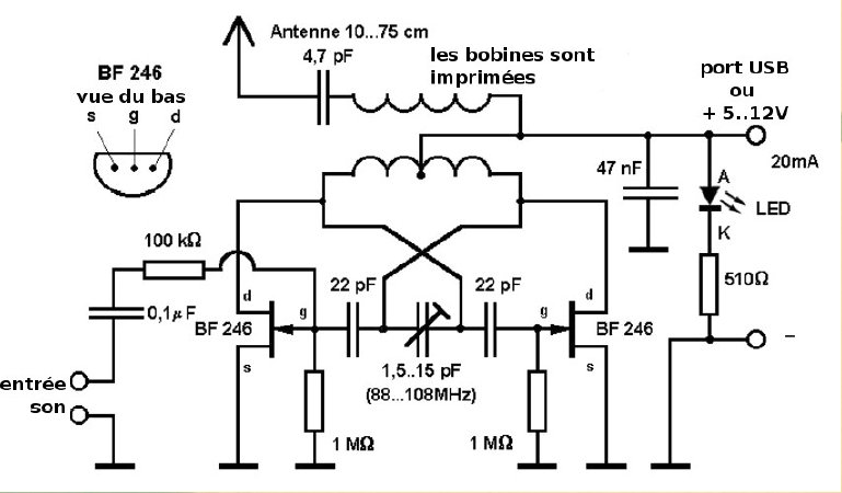
This compact FM transmitter is designed for connection to a USB port and has a range of approximately 50 meters. It can be utilized alongside multiple mini-transmitters to create a diverse and engaging radio program. The power supply through...
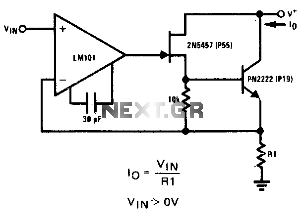
The 2N5457 JFET and PN2222 bipolar transistor exhibit high output impedance. Employing Rl as a current sensing resistor to feedback into the LM101 operational amplifier yields significant loop gain for negative feedback, thereby improving the circuit's capability as a...
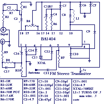
You'll find that this is a very easy project to build. It will transmit good quality sound in the FM band (88 - 108 MHz). One important item is that the IC chip operates on 3 volts DC. The...