
Push Button ON-OFF Soft Latch Circuits

Utilizing a single tactile switch button to alternately toggle a circuit ON and OFF necessitates a circuit that incorporates a bistable logic latch. This latch can be realized using a D flip-flop or through positive feedback involving two inverting amplifiers or logic gates. For instance, a basic latching ON-OFF switch can be constructed using a dual NAND gate, where a brief button press toggles the output state of the NAND gate latch. Any CMOS NAND gate, including Schmitt trigger gates, can be employed, and other inverting devices such as hex inverters, open collector inverters, NAND or NOR gates, transistors, FETs, or MOSFETs can also be utilized with minor circuit modifications.
Upon initial power application, a capacitor at the input of the first gate ensures that the latch output, Vout, is initially latched low. Subsequent button presses toggle the output between high and low states. This circuit requires only a single active component, the surface mount dual MOSFET, yet it can switch currents of up to 4 Amps. The load may include a variety of electrical devices, ranging from high-power LED lights to the power supply for embedded computers.
However, placing the high-side MOSFET switch within the feedback path of the latch can introduce a potential failure when the output drives slow-decay capacitive loads, which is common in power bus switch applications. If the switch supplies power to a power supply with large input capacitors, and the load does not draw sufficient current for those capacitors to discharge quickly, the transient button press may not reliably turn OFF the switch. After the high-side switch turns OFF, the sustained voltage at its output, maintained by the large capacitors, may keep the lower MOSFET turned ON, inadvertently reactivating the high-side switch upon button release.
In applications involving smart products with microcontrollers, it is often necessary to ensure that power is not accidentally removed. Therefore, a power switch that can be activated by a brief button press but requires a longer, intentional button hold to deactivate is desirable. This design prevents unintentional power loss from accidental touches to the tactile switch.
The circuit operates as follows: Upon the initial application of power, the source-gate voltage of the P-FET either remains at zero, keeping the high-side switch OFF, or the gate is held low as the source voltage rises, turning on the MOSFET, contingent upon the position of the Auto-ON jumper. When the MOSFET is OFF, a momentary press of the ON/OFF button pulls the gate low for tens of milliseconds, fully activating the high-side MOSFET. The resulting output voltage rise is transmitted to the N-MOSFET's gate through a 10 µF capacitor and resistors, turning it ON. With the low-side FET activated, the gate of the high-side FET is pulled low, maintaining its ON state. Consequently, the power remains latched ON even after the button is released, as only a few volts of VGS are sufficient to keep the MOSFETs fully ON.
To turn the circuit OFF, a prolonged button press is required. Holding the button down pulls the gate of the low-side MOSFET low after a delay determined by the discharge of the 10 µF capacitor through a 300 kΩ resistor. This action turns OFF the low-side MOSFET, allowing the gate of the high-side MOSFET to rise, ultimately deactivating the circuit.This page provides soft power switch circuits for toggling electronic devices ON and OFF with a momentary button press that controls a latching high-side MOSFET power switch. Several micropower latching switch circuits are provided. Owing to their low current in the OFF state, they`re well suited to battery operated portable instruments.
Feel free to use these circuits as is, or modify them for your needs, wherever you might need a power bus switch circuit. The soft power switch circuit designs shown on this page provide both functions. You may also be interested in ON/OFF switches that limit capacitor in-rush currents, or switches to specifically turn ON/OFF microcontroller products.
Using a single tactile switch button to alternately toggle a circuit ON and OFF requires a circuit containing a bistable logic latch. Such a latch can be implemented using a D flop flop, or by using positive feedback around any two inverting amplifiers or logic gates.
For example, a basic latching ON-OFF switch can be implemented using a dual NAND gate, using this circuit: A brief button press toggles the output state of this NAND gate latch. Any CMOS NAND gate can be used, including Schmitt trigger gates. In fact, any inverting devices can be used with minor changes to the circuit: a hex inverter, open collector inverters, NAND or NOR gates, transistors, FETs or MOSFETs.
When power is first applied, the capacitor at the input of the first gate guarantees that the latch output, Vout, is initially latched low. Thereafter, button presses toggle the output high and low. This circuit uses only a single active device, the surface mount dual MOSFET, yet toggles ON and OFF currents of up to 4 Amp.
The load may be just about any electrical device, from high power LED lights to the power supply of embedded computers. Placing the high side MOSFET switch within the feedback path for the latch does introduce a potential failure if the output drives slow-decay capacitive loads, as it might in power bus switches.
If the switch applies power to a power supply with large input capacitors, and the load does not draw enough current for those capacitors to discharge quickly, then the transient button press may not turn OFF the switch reliably. Instead, after the high-side switch turns OFF, the sustained voltage at its output, propped up by the large capacitors, keeps the lower MOSFET turned ON, which in turn activates the high side switch after the button release.
For controlling smart products containing microcontrollers you often want to ensure that the power is not inadvertently removed. Consequently, you want a power switch that can be turned ON by a brief button press, but requires a longer, deliberate button hold to turn it OFF.
That prevents accidentally killing power if the tactile switch is unintentionally touched. Circuit operation is as follows: When power is first applied, the source-gate voltage of the P-FET either remains zero, keeping the high side switch OFF, or the gate is held low as the source rises, turning on the MOSFET, depending on the position of the Auto-ON jumper. When the MOSFET is OFF, a momentary touch of the ON/OFF button pulls the gate low for tens of milliseconds, fully turning on the high side MOSFET.
The output voltage rise is transmitted to the N-MOSFET`s gate through the 10 F capacitor and resistors, turning it ON. With the low-side FET ON, the gate of the high-side FET is pulled low, keeping it turned ON. Consequently, the power latches ON even after the button is released. Only a few volts of VGS is sufficient to keep the MOSFETs turned fully ON. Subsequently, a long button touch turns the circuit OFF. Pressing and holding the button down pulls down the gate of the low-side MOSFET after a few second delay determined by the discharge of the 10 F capacitor through the 300 k © resistor.
The low-side MOSFET turns OFF, allowing the gate of the high-side MOSFET to rise t 🔗 External reference
Related Circuits
High Power Siren Circuit. This article discusses a robust siren circuit suitable for various applications. A complementary transistor pair (BC557 & BC337) is configured as an oscillator to directly drive the speaker. Transistor Q1 (BC557) is utilized to ensure...
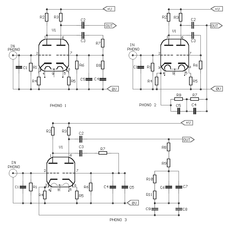
The three circuits were based on the vacuum tube ECC83, designed to produce phono preamplifiers in compliance with RIAA standards. The described circuits utilize the ECC83 vacuum tube, a dual-triode component known for its low noise and high gain characteristics,...
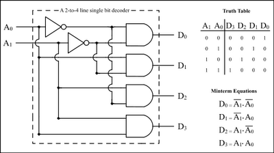
The Encoder and Decoder are different types of combinational circuits used to convert binary information to decimal, octal, and hexadecimal formats, and vice versa. A decoder is a combinational circuit that converts n-bit binary information into 2^n unique outputs....
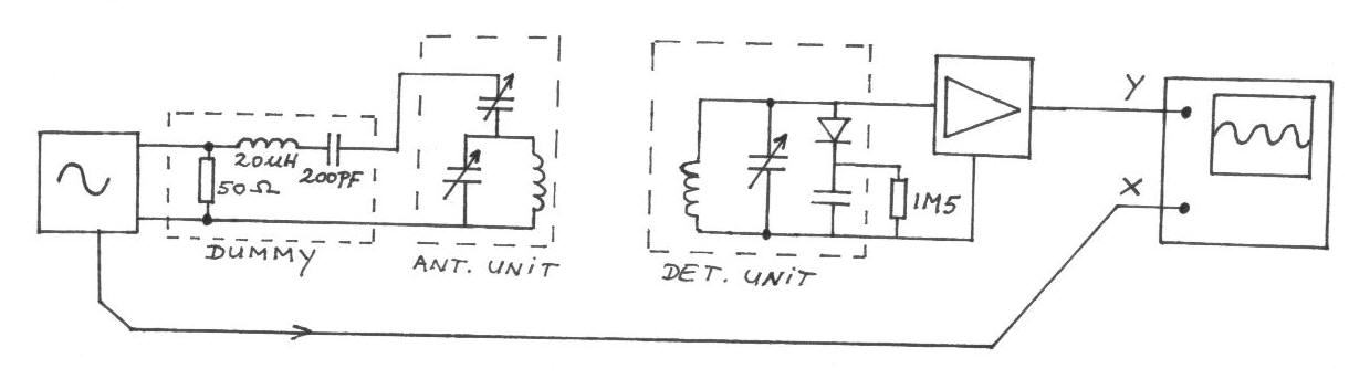
The frequency remains constant, oscillating between two predetermined values. On the oscilloscope display, a frequency spectrum is observed, showcasing the response curves of the two circuits. The input voltage of the receiver is 0.1 Volt peak-to-peak, while the voltage...
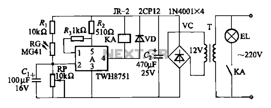
The adjustment potentiometer RP can modify the sensitivity of the device. Capacitors C1 function as an anti-light interference mechanism for instantaneous action. The adjustment potentiometer (RP) is a variable resistor that allows for fine-tuning of the device's sensitivity. By altering...
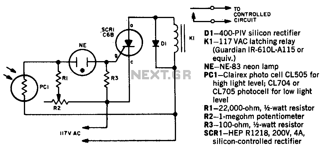
When a beam of light strikes the photocell, the voltage across the neon lamp NE-1 rises sharply. NE-1 turns on and triggers the SCR. K1 is an impulse relay whose contacts remain in position even after the coil current...