
Regulated 12 Volt Supply

The circuit described operates on the principle of voltage regulation through the use of a zener diode in conjunction with a transistor amplifier. The 13-volt zener diode, D2, establishes a stable reference voltage. When the input voltage exceeds the zener breakdown voltage, the diode conducts and maintains the output voltage at approximately 12.3 volts after accounting for the voltage drop across the transistor's base-emitter junction.
The transistor serves to amplify the current capacity of the circuit, allowing it to deliver up to 500 mA to the load. This capability is essential for applications requiring a stable voltage supply for various electronic components. The configuration typically includes additional components such as resistors for biasing the transistor and capacitors for filtering to ensure stability and reduce noise in the output voltage.
In designing this circuit, careful consideration must be given to the selection of the zener diode and transistor to ensure they can handle the required voltage and current ratings. Additionally, heat dissipation mechanisms may be necessary, particularly if the circuit operates near its maximum load for extended periods, as both the zener diode and transistor can generate heat during operation. Proper thermal management will help maintain the reliability and longevity of the circuit.This circuit above uses a 13 volt zener diode, D2 which provides the voltage regulation. Aprroximately 0. 7 Volts are dropped across the transistors b-e junction, leaving a higher current 12. 3 Volt output supply. This circuit can supply loads of up to 500 mA. This circuit is also known as an amplified zener circuit. 🔗 External reference
Related Circuits

This is an application circuit for calibration known as a high voltage AC calibrator circuit. A key aspect of sine wave oscillator design is the stable control of amplitude. In this circuit, the amplitude is stabilized through servo control,...
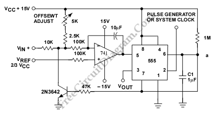
This is a circuit for a Voltage-to-Pulse Duration Converter. The circuit is designed to convert voltage into pulse duration by integrating a timer IC and an operational amplifier (OP Amp). The Voltage-to-Pulse Duration Converter circuit utilizes a timer IC, typically...
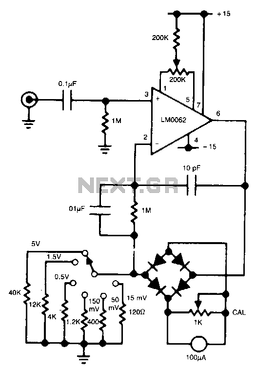
In this circuit, a diode bridge is utilized as a meter rectifier. The offset voltage is compensated for by the operational amplifier, as the bridge is part of the feedback network. The circuit employs a diode bridge rectifier, which consists...

The photodiode current-to-voltage converter circuit employs three CA3130 BiMOS operational amplifiers, designed for applications that require sensitivity to sub-picoampere input currents. This circuit generates a ground-referenced output voltage that is directly proportional to the input current flowing through the...
This circuit can be adapted for other regulated and unregulated voltages by using different regulators and batteries. For a 15 Volt regulated supply use two 12 Volt batteries in series and a 7815 regulator. There is a lot of...

I use this power supply for applications that doesn't use too mucho power. It can provide power to circuit that uses less than 100mA without any problem. The disadvantage of this circuit is the danger of an electrical shock,...