
Regulator Circuit

The circuit described utilizes the LM317 adjustable voltage regulator, which is capable of outputting voltages from 1.25 V up to 37 V, with the added capability of reaching 0 V through the use of a zener diode and an op amp configuration. The zener diode serves to establish a stable reference voltage, which is essential for the accurate regulation of the output voltage. In the traditional setup (as shown in Figure 74-1 (a)), the zener diode directly influences the reference voltage of the LM317, providing a negative feedback loop that stabilizes the output.
In the alternative configuration (Figure 74-1 (b)), the operational amplifier is employed to enhance performance, particularly in low-voltage applications. This configuration allows for more precise control over the output voltage by measuring the voltage drop across resistor R1 and inverting this signal to create a negative reference voltage. The differential amplifier setup ensures that any fluctuations in the reference voltage have a minimized effect on the output, which is particularly beneficial when operating at lower voltages.
The choice of op amp can influence circuit performance; while a standard 741 op amp suffices for basic applications, the LF356 offers enhanced bandwidth and lower noise characteristics, which can be advantageous in precision applications. The design also incorporates a center-tapped mains transformer to provide the necessary negative supply voltage for the op amp, ensuring that the circuit operates effectively across its intended voltage range.
Overall, this circuit design exemplifies a robust solution for applications requiring adjustable voltage regulation down to 0 V, combining the reliability of the LM317 with the precision of an op amp in a differential configuration. The prototype results indicate that this approach is effective, making it suitable for a variety of electronic applications where precise voltage regulation is required. The special characteristic of this regulator is that the output voltage can be adjusted down to 0 V. The regulation is pr ovided by an integrated regulator Type LM317. As is normal in supplies that can be adjusted to 0 V, this IC is used in conjunction with a zener diode. This diode provides a reference voltage that is equal, but of opposite sign, to the reference voltage (U,) of the regulator, as shown in Fig.
74-1 (a). Potential divider R1/R2 enables the output voltage to be adjusted. In this circuit, the negative reference voltage is derived in a different manner: from the regulator with the aid of an op amp (Fig. 74-1 (b)). The op amp is connected as a differential amplifier that measures the voltage across Rl and inverts this voltage to Ur.
An additional advantage of this method is that at low-output voltages, a change in the reference voltage has less effect on the output voltage than the circuit in Fig. 74-1 (a). The prototype, constructed as shown in Fig. 74-1 (c), gave very satisfactory results. The op amp need not meet any special requirements: a 741 works fine, although an LF356 gives a slightly better performance.
The negative supply for the op amp can be obtained with the aid of a center-tapped mains transformer.
Related Circuits
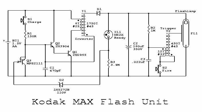
This flash circuit is a typical camera flash. This flash circuit functions as a high-voltage power supply for camera flash units, enabling the rapid discharge of energy to produce a bright flash of light. The primary components of a typical...
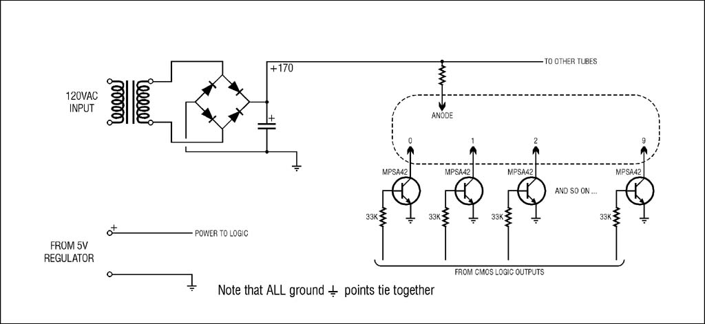
The high voltage supply will function, but for safety and to prevent accidental damage during troubleshooting with an oscilloscope, it is highly recommended to use an isolation transformer on the 120VAC input. A small 1:1 transformer rated at 30VA...

The following circuit illustrates a simple infrared sensor module circuit diagram. Features include a simple infrared sensor module and flame detection. The simple infrared sensor module circuit operates by utilizing an infrared (IR) transmitter and receiver pair. The IR transmitter...
This simple circuit is started running by connecting a twelve volt battery across the terminals, causing the large diameter Light-Emitting Diode to light up. When the battery is removed, the LED stays lit up because the circuit has become...
This circuit consists of three single-junction transistor time relay circuits utilizing a pulse charging mechanism, allowing for extended delay times of up to several minutes. The first stage delay circuit incorporates unijunction transistors (VTi) and other components, where capacitor...
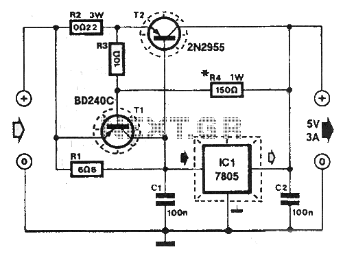
At this voltage regulator prototype the maximum current, with output shortcircuited it was only 0.5 A, so no overheating occurred. In this DC voltage regulator circuit, T1 is for current limitation. As soon as the voltage on the R2...