
AM circuit by MC1496
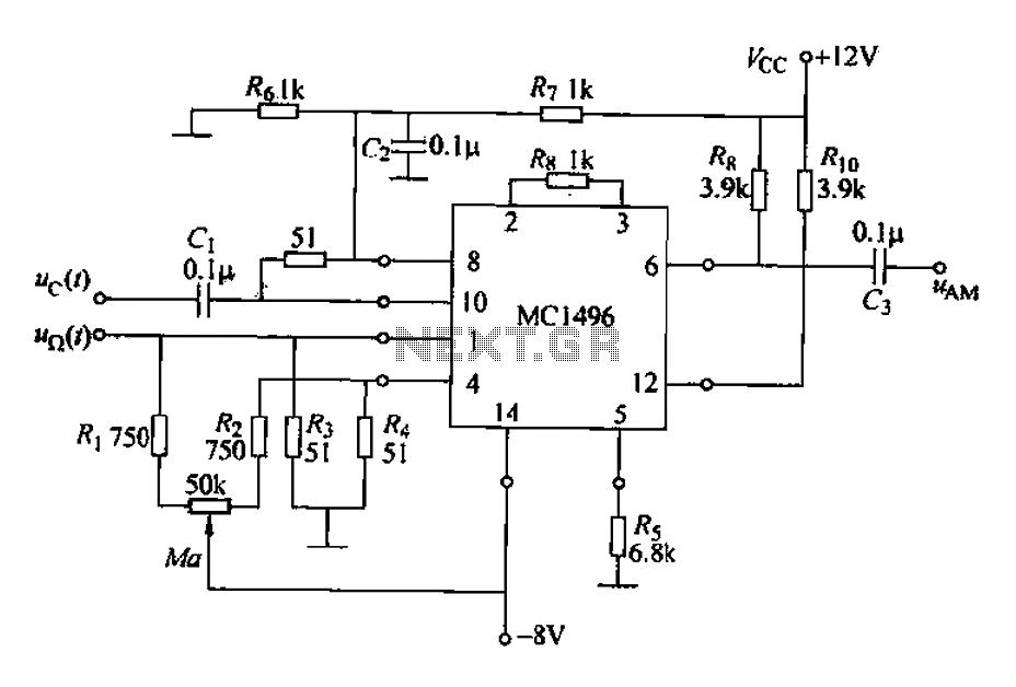
The AM MC1496 analog multiplier integrated circuit is designed for applications involving amplitude modulation, particularly in communication systems where signal integrity is crucial. The circuit operates by utilizing two input channels, allowing for the modulation of a carrier signal. The configuration ensures that the DC bias level is correctly set to 6V, which is vital for the proper functioning of the multiplier.
The Y input is particularly important as it allows for the superimposition of an AC modulation signal onto the DC input voltage. By employing a potentiometer, users can finely tune the modulation index, which directly affects the depth of modulation and, consequently, the quality of the transmitted signal. This tuning capability is essential in optimizing the performance of the modulation process.
The output of the circuit is connected to a bandpass filter, which is crucial for isolating the desired frequency components of the modulated signal while attenuating unwanted frequencies. The tuning of this filter is aligned with the carrier frequency, ensuring that the output signal maintains its integrity and is suitable for further processing or transmission.
Negative feedback is implemented through a resistor connected to the Y channel, which stabilizes the circuit and enhances linearity. This feedback mechanism is important for reducing distortion and improving the overall performance of the modulation process.
To achieve precise control over the input signal levels, the potentiometer is adjusted to maintain a zero DC potential difference at the Y channel. This adjustment allows only the AC modulation signal to pass through, ensuring that the output is a clean representation of the desired modulated signal.
In scenarios where the potentiometer's current needs to be minimized for accurate adjustments, the addition of two 750Ω resistors is recommended. This configuration helps in reducing the load on the potentiometer, facilitating easier and more accurate tuning to achieve the desired modulation characteristics.
Overall, the AM MC1496 integrated circuit configuration as described offers a robust solution for amplitude modulation applications, providing flexibility in tuning and ensuring high-quality signal transmission.AM MC1496 analog multiplier integrated circuit configuration shown in Figure 21-39. Channel two-input, ? pin DC bits are 6V, can be used as a carrier channel two input channels } Y input O, feet between external have zero circuit, by adjusting potentiometer allows 50kn potential than O foot foot high Uy, the modulation signal u ( ) is superimposed with the DC input voltage UY Y channel. Adjust the potentiometer to change the modulation index Ma. Output terminal, feet to bandpass filter tuned to the carrier frequency., feet between the outer negative feedback resistor connected to the Y channel.
The circuit shown indiscriminately 21-39 double-sideband amplitude modulation circuit can be composed, adjust the potentiometer is intended to make the Y channel O, feet between the DC potential difference is zero, the Y-channel input signal only the AC modulation signal. In order to reduce the current flowing through the potentiometer, accurate and easy to zero, can increase two 75051 resistor, such as increased each lOkn.
Related Circuits
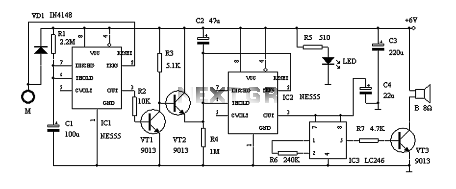
This circuit describes a door alarm system equipped with a time recognition feature. When the owner opens the door, it remains in a normal state for approximately 30 seconds without triggering the alarm. However, if the door is opened...

Figure 1-30 illustrates an example of an output capacitor-less (OCL) power amplifier circuit, which can be analyzed as follows: In this circuit, transistors VTi and VTz form a single-ended input and a differential input single-ended output amplifier configuration. The...
Ensure that connections are verified against the circuit diagram and schematic provided below. This can be utilized while following the tutorial video. The circuit diagram serves as a crucial reference for accurately assembling electronic components in a project. It illustrates...

This functioning radio was built for an electronics module. The specified design was modified to include batteries, a switch, and a speaker instead of headphones. An additional amplifier circuit was required to power the speaker driver. Although not necessary,...
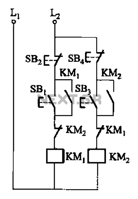
A, B, and two electric motors allow simultaneous operation through interlock control. The two motors can be connected in series with each other using normally closed contacts in the respective coil circuit. The circuit design facilitates the interlocking operation of...

The simple pulse width modulation circuit is illustrated in the figure. It utilizes an operational amplifier to create a multivibrator, resulting in a symmetrical oscillation output signal with a duty cycle of 50%. By adjusting the external threshold voltage,...