
Full-band phase locked loop circuit diagram fast

The presented circuit diagram outlines a phase-locked loop (PLL) configuration that integrates an AM686 latched comparator functioning as the voltage-controlled oscillator (VCO). This VCO is pivotal in generating a frequency output that is dependent on the input voltage. The circuit also incorporates a TTL latch, which is crucial for producing edge-triggered comparisons. This arrangement allows for precise synchronization of the output frequency with a reference frequency.
In this PLL design, the low-pass filter plays a significant role in smoothing the output signal from the VCO. The components R1, R2, and C2 are arranged to form a filter that effectively reduces high-frequency noise, ensuring that only the desired frequency components are passed through. The low-pass filter's cutoff frequency can be adjusted by selecting appropriate values for R1, R2, and C2, which directly influences the loop's stability and response time.
The operation of the PLL involves the VCO generating a signal that is compared to a reference signal. The edge-triggered comparators, enabled by the TTL latch, facilitate this comparison by detecting the phase difference between the two signals. The output of the comparator is then fed back to the VCO, adjusting its frequency to minimize the phase difference. This feedback mechanism is essential for maintaining lock and achieving stable frequency output.
Overall, this PLL circuit is designed for applications requiring precise frequency control and stability, making it suitable for various electronic systems where synchronization of signals is critical.A circuit diagram of a phase locked loop fast the whole band takes a Am686 latched comparator as voltage controlled oscillator, and the other with a TTL latch coupled to genera te edge-triggered comparators. VCO and comparison with the low-pass filter R1, R2, C2 link, constitute PLL.
Related Circuits
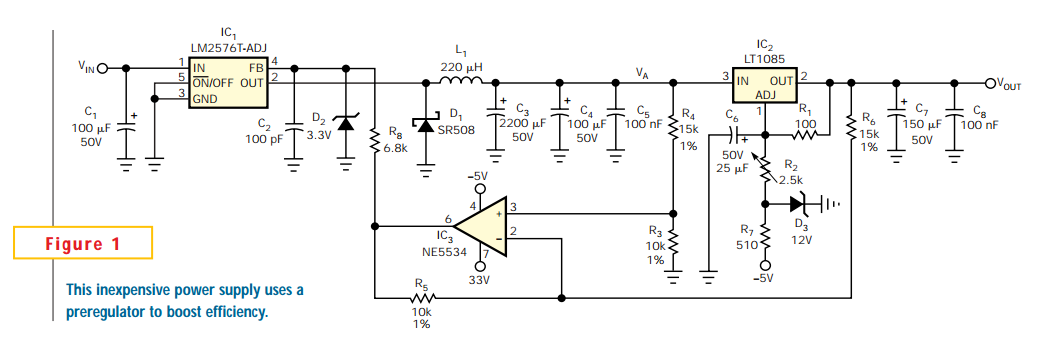
Linear regulators are easy to implement and have better noise and drift characteristics than switching approaches. Their largest disadvantage is inefficiency: excess energy dissipated as heat. Several well-known techniques are available to minimize the input-to-output voltage across a linear...

The circuit diagram of a simple capacitance meter is presented here. The primary component of this circuit is the frequency-to-voltage converter. The simple capacitance meter circuit utilizes a frequency-to-voltage converter as its central element to measure capacitance values. This circuit...

The article presents a circuit that can be used for indicating the riding speed of a bicycle. The bicycle speedometer circuit explained here utilizes standard components such as transistors and LEDs to effectively display a clear 10-step, accurately calibrated...
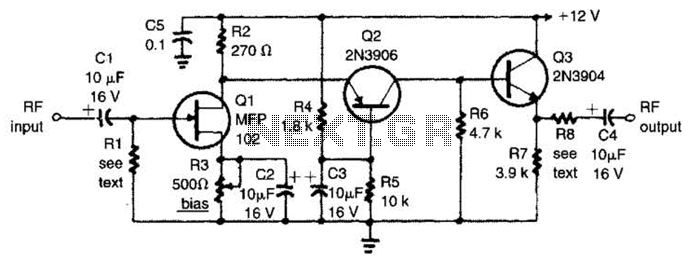
The circuit features a frequency response that spans from 100 Hz to 3 MHz, with a gain of approximately 30 dB. Field-effect transistor Q1 is arranged in a common-source self-biased configuration, and an optional resistor R1 is available to...
A composite pipe can be reduced to facilitate the adjustment of the control current within the tube. Composite pipes are often utilized in various applications due to their lightweight, strength, and flexibility. When discussing the reduction of a composite pipe,...
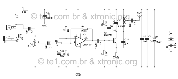
Evolution FM transmitter utilizing a 2N2218 transistor with an audio amplification stage using an LM741 operational amplifier. The design accommodates audio input from various sources such as MP3 players, MP4 devices, mobile phones, computers, and other audio sources, surpassing...