
Sawtooth generator circuit

The sawtooth wave generator circuit utilizing a 555 timer IC is designed to produce a linear ramp output waveform, suitable for various applications such as signal processing, waveform generation, and modulation. The circuit primarily consists of a 555 timer configured in astable mode, a capacitor (C), a resistor (R), and a diode (1N4001) for output stabilization.
The operation begins with the capacitor (C) in a fully discharged state, resulting in zero voltage across it. This condition triggers the internal comparators of the 555 timer, specifically the one connected to pin 2. As a result, the output of the timer goes high, activating an internal transistor that allows the capacitor to charge towards the supply voltage (Vcc). The charging process continues until the voltage across the capacitor reaches approximately 2/3 of Vcc.
At this threshold, the output of the 555 timer switches low, causing the internal transistor to short the capacitor to ground, leading to a rapid discharge of the capacitor. The discharge continues until the voltage across the capacitor drops below 1/3 of Vcc. Once this condition is met, the 555 timer output returns to a high state, and the cycle repeats. This charging and discharging cycle results in a sawtooth waveform output, with the frequency of oscillation determined by the values of R, C, Vpp, and Vcc.
The frequency of the sawtooth wave can be calculated using the formula f = (Vcc - 2.7) / (R * C * Vpp). Here, Vcc represents the supply voltage, while Vpp indicates the desired peak-to-peak voltage of the output waveform. Proper selection of R, C, Vpp, and Vcc values is essential to achieve the desired frequency output, allowing for flexibility in the design to meet specific application requirements.
The inclusion of the 1N4001 diode ensures that the output voltage across the capacitor does not exceed ground level, thereby protecting downstream components from potential over-voltage conditions. This characteristic is particularly important in applications where precise voltage levels are critical. Overall, the 555 timer-based sawtooth wave generator offers a simple yet effective solution for generating linear ramp signals in various electronic applications.Sawtooth wave generators using opamp are very common. But the disadvantage is that it requires a bipolar power supply. A sawtooth wave generator can be built using a simple 555 timer IC and a transistor as shown in the circuit diagram. The working of the circuit can be explained as follows: The part of the circuit consisting of the capacitor C, transistor,zener diode and the resistors form a constant current source to charge the capacitor.
Initially assume the capacitor is fully discharged. The voltage across it is zero and hence the internal comparators inside the 555 connected to pin 2 causes the 555's output to go high and the internal transistor of 555 shorting the capacitor C to ground opens and the capacitor starts charging to the supply voltage. As it charges, when its voltage increases above 2/3rd the supply voltage, the 555's output goes low, and shorts the C to ground, thus discharging it. Again the 555's output goes high when the voltage across C decreases below 1/3rd supply. Hence the capacitor charges and discharges between 2/3rd and 1/3rd supply. Note that the output is taken across the capacitor. The 1N4001 diode makes the voltage across the capacitor go to ground level (almost). The frequency of the circuit is given by: f = (Vcc-2.7)/(R*C*Vpp) where: Vcc= Supply voltage.
Vpp= Peak to peak voltage of the output required. Choose proper R,C,Vpp and Vcc values to get the required 'f' value. 🔗 External reference
Related Circuits
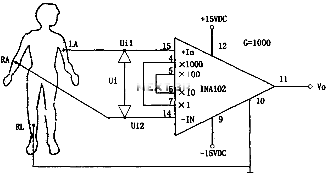
This document outlines a preamplifier circuit designed for measuring human biological signals, such as ECG and EEG. These biological signals are typically weak and require high amplification circuits. The circuit utilizes a low-power integrated operational amplifier, INA102. The INA102...
For example, I do not understand the process of demodulation or the modulation itself, and so on. Is there someone who can understand this circuit? Could you please assist me? The circuit in question likely involves a modulation and demodulation...

To utilize this facility, the calling subscriber must first dial the standard phone number of the intended recipient. Once the call is connected, the calling party does not hear a ring-back tone. The calling subscriber must then press the...

This inverter is designed to operate appliances such as TVs and stereos while traveling or camping. It converts 12 VDC to 120 VAC, with the output wattage determined by the transistors used for Q1 and Q2, as well as...
An electronic dice is a classic introductory project for individuals interested in electronics. It consists of a timer, counter, and several LEDs, forming a circuit that adds an engaging element to traditional board games. When the switch is activated,...
A fast pulse detector can be constructed using this circuit. A very fast input pulse will surpass the amplifier's slew rate, resulting in a prolonged overload recovery time. Implementing some degree of dv/dt limiting on the input can alleviate...