
Small low-frequency drift polarity switching synchronous detector circuit
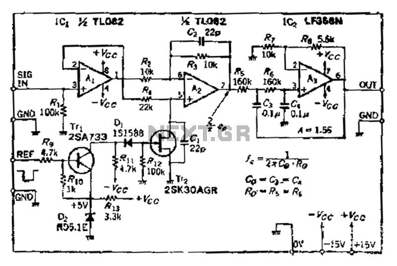
An electronic circuit utilizing a PNP transistor as a switch or amplifier can be designed based on the described operation. The circuit consists of a PNP transistor (Tr) configured in a common-emitter configuration. The emitter of the transistor is connected to +5V, while the collector is linked to the load, which may be a diode (Dj) and a resistor (Rz) in series. The base of the transistor receives a control signal from a TTL logic level input, which determines the on/off state of the transistor.
When the TTL input is high (logic 1), the base current flows into the transistor, turning it on and allowing current to flow from the emitter to the collector. This causes the output voltage at the collector to rise close to +5V, effectively turning off the diode Dj. Conversely, when the TTL input is low (logic 0), the base current ceases, and the transistor turns off, resulting in the collector voltage dropping towards ground potential, which allows diode Dj to conduct if the load conditions permit.
The analog switching circuit can be further refined by integrating a CMOS analog switch for applications requiring lower power consumption and higher switching speeds. However, the selection of components must be balanced with cost constraints, as CMOS devices may be more expensive than traditional bipolar junction transistors (BJTs).
Overall, this circuit configuration provides a reliable method for controlling analog signals using digital logic levels, enabling seamless integration into larger electronic systems. Proper attention to component specifications and circuit layout will ensure optimal performance and reliability in various applications.After TT2 off, the input signal input via chi Az, dry white [input resistance is very high, becomes the same potential, the inverting input terminal must also be associated wit h the move, so Trr play the role of a magnification of the follower 1. Analog switching circuit Tr soap must be formed between the gate electrode a source off when the voltage v. J negative direction placed near the center off voltage vP. To use TTL level drive, the + s/ov replaced - vcc/+ Sv, in addition can also be replaced C-MOS analog switch, but must consider the cost element.
Tr. It is a PNP transistor, the emitter potential of Sv, T TL input power when oH- almost off, then set the telegraph voltage - vcc (TT2 so disconnected). TTL level input as labor hours, so that Tr, produce base current, r, conduction, the collector potential placed near + sv, diode Dj off, then v accounted s FO, rz turned on.
Related Circuits
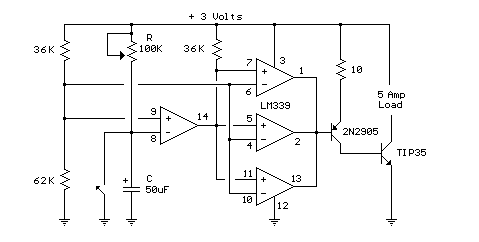
This circuit utilizes an LM339 quad voltage comparator to create a time delay and manage a high current output at low voltage levels. Approximately 5 amps of current can be sourced using a pair of fresh alkaline D batteries....

This circuit separates an input voltage signal into its components: (1) the absolute value and (2) the polarity or 'sign' (+ or -). It is designed to handle direct current (DC) signals. The circuit operates by utilizing operational amplifiers (op-amps)...
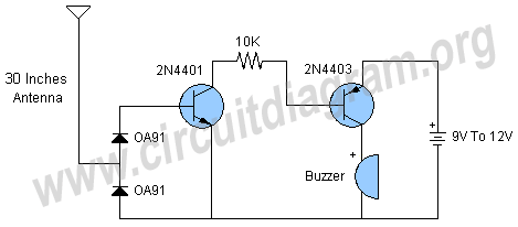
Similar to a field strength meter, an RF detector circuit serves as a valuable project for detecting nearby RF signals. The circuit presented here is capable of detecting a wide range of RF frequencies and provides an alarm when...

The power supply presented is intended to function with a wall transformer. This circuit can be utilized alongside a variable supply for testing circuits in a laboratory setting. T2 serves as a 12-V wall transformer. The power supply circuit is...
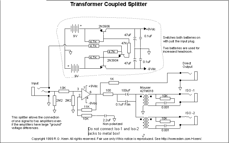
An active amplified transformer isolated signal splitter that enables a hum-free connection of one guitar to multiple amplifiers, while also providing a direct output. This includes a discussion on using audio transformers for equipment interconnections and mentions line-level transformers...
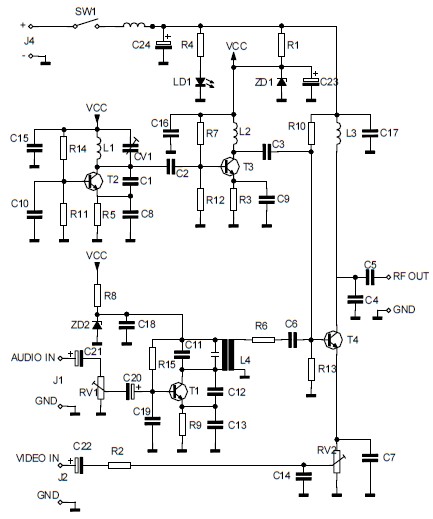
The circuit converts audio and video signals into a UHF TV signal, allowing a video signal from a camera or other source to be connected to a standard TV set. The audio and video signals are transformed into a...