
Simple Analog Multiplier Circuit Using LM107

The described circuit functions as an analog multiplier, which is essential in various applications such as signal processing and control systems. The core of the circuit utilizes a controlled gain amplifier, designated as A2, which adjusts the gain based on the input signals. This enables the circuit to perform multiplication of two analog signals effectively.
In this configuration, the analog multiplier can be realized using operational amplifiers (op-amps) configured in a specific arrangement. The log-antilog circuit is crucial for achieving the multiplication function, as it converts the input voltages into logarithmic values, allowing for the addition of these logarithmic signals. The summing junction, typically formed by an inverting amplifier, facilitates the addition of the logarithmic inputs.
Photoconductors may be integrated into the circuit to enable light-controlled operations, where the resistance of the photoconductor changes with light intensity, thereby affecting the gain of the amplifier. This feature allows for the modulation of the output based on ambient light conditions, making the circuit versatile for applications in light-sensitive environments.
Overall, the design and implementation of this analog multiplier circuit showcase the principles of analog signal processing, leveraging the characteristics of operational amplifiers and logarithmic functions to achieve accurate multiplication of input signals.This circuit a simple analog multiplier, the circuit operation may be understood by considering A2 as a controlled gain amplifier, Analog Multiplier, Multiplier Circuit, log-antilog circuit, analog multiplication, controlled gain amplifier, summing junction, photoconductors, inverting amplifier,. 🔗 External reference
Related Circuits
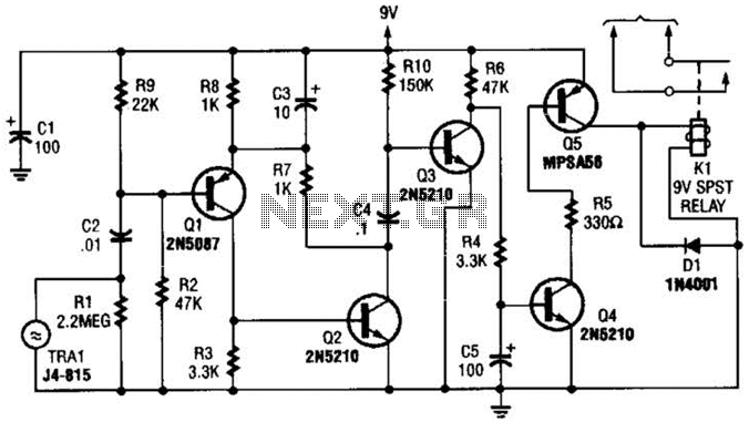
A GC Electronics P/N J4-815 transducer is utilized to receive 40-kHz acoustic remote-control signals. The receiver activates a relay to control another circuit. The GC Electronics P/N J4-815 transducer is designed specifically for the reception of 40-kHz acoustic signals, which...

The TDA6106Q test circuit, as depicted in the provided figure, operates with a feedback factor of 1/116. The input signal, Vin, is received from the input network consisting of resistors R1, R9 and capacitors C1, C2. The TDA6106Q IC...
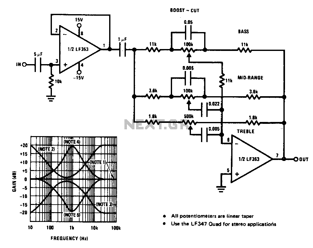
A simple single-transistor circuit provides an approximate 15 dB boost at 100 Hz and a 15 dB cut at 15 kHz. A low-noise audio transistor is utilized, and the output can be directly connected to any existing amplifier volume...

This circuit is beneficial for applications where a load must be activated from one location and deactivated from another. Multiple momentary normally open (N/O) switches or push buttons can be connected in parallel. The circuit described facilitates remote control of...
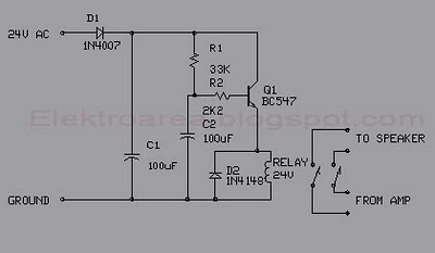
This circuit was designed for an audio amplifier project to control the speaker output relay. The primary function of this circuit is to manage the relay that activates the speaker output in the audio amplifier. The circuit introduces a...
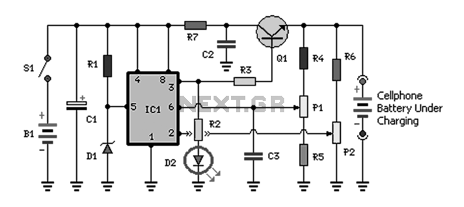
Charging a mobile phone or cellphone battery presents a significant challenge while traveling, as a power supply source is often not readily available. If the cellphone remains switched on continuously, its battery can deplete within five to six hours,...