
Simple DC power delay circuit

The described DC power delay circuit is designed to control the timing of power delivery to a load by employing an SCR and a Zener diode in its operation. The main components of the circuit include a power source, a capacitor (C2), a resistor (R2), an SCR (H1), and a Zener diode (D3).
When the circuit is powered, the capacitor C2 begins to charge through resistor R2. The charging time is determined by the values of R2 and C2, which dictate the RC time constant of the circuit. As the capacitor charges, its voltage increases steadily until it reaches the breakdown voltage of the Zener diode D3. At this point, D3 conducts and provides a gate pulse to the SCR H1, turning it on.
Once SCR H1 is triggered, it allows current to flow from the power source to the load connected at the OUT terminal. The delay in power delivery is determined by the time it takes for the capacitor to charge to the Zener breakdown voltage, effectively controlling when the load receives power. This feature makes the circuit suitable for applications where a delay is required, such as in lighting systems, motor control, or other electronic devices that require sequential power-up.
The design of this circuit should consider the specifications of the components used, including the voltage rating of the capacitor, the power rating of the resistor, and the current handling capability of the SCR to ensure reliable operation under the intended load conditions. Additionally, proper heat sinking for the SCR may be necessary depending on the load current to prevent thermal overload.The circuit diagram shown here is of a simple DC power delay circuit that is based on an SCR. This circuit is a very handy one and can be employed in many applications. The working of this circuit is very simple. When the input power is applied the capacitor C2 charges through resistor R2 and when the voltage across the capacitor just exceeds the Zener diode D3`s breakdown voltage, it breaks down and the SCR H1 is triggered and the delayed power will be available at the delayed OUT terminal. 🔗 External reference
Related Circuits
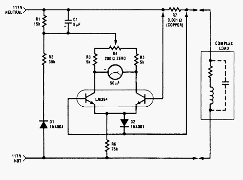
This wattmeter circuit has a measurement range of up to 1 kW. It is capable of providing complete (X)(Y) function with the use of only one transistor. The circuit is designed for operation with 117 Vac ±50 Vac. Modifications...
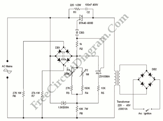
A typical circuit for welding equipment is illustrated in the following circuit diagram. The turn-on delay can be accurately controlled with Potentiometer P2, allowing for effective discharge management. The welding equipment circuit typically incorporates several key components to ensure proper...
If the transmitter stick-potentiometer delivers a voltage about 2 - 3 V, this circuit will be suitable. If you want to avoid using the battery cable (supplying Vcc for IC1 and -2), you can use a separate 5V supply...
The multifunction circuit primarily refers to its capability to operate in three modes: "delayed pull," "time release," and "delayed cycle." The term "delay" indicates that the relay is energized after a predetermined time; however, the relay does not activate...
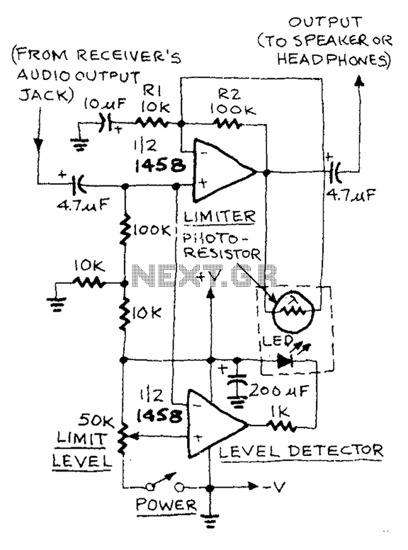
The AUD.LIMITER circuit features a level trim potentiometer that allows for adjustment of the limiting level. When the input signal exceeds the set level of the potentiometer, the output from one half of the operational amplifier, functioning as a...
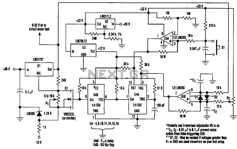
When testing a circuit, a variable voltage source with overvoltage shutdown capabilities is highly beneficial. In this circuit, resistor R1 is adjusted to a value 1 to 2 volts below the eventual shutdown threshold. Resistor R2 is responsible for...