
Simple Monostable Flip Flop

The monostable flip flop, or one-shot circuit, is a fundamental building block in digital electronics, primarily used for generating precise timing pulses. This circuit operates in a single stable state and transitions to a temporary state upon receiving a triggering signal. The operation can be understood through the interaction of transistors, capacitors, and resistors.
In a discrete implementation of the monostable flip flop, two transistors are employed—one in a conducting state (active) and the other in a non-conducting state (inactive). The left transistor is typically in a conducting state, allowing current to flow, while the right transistor remains off. The circuit is activated by pressing a switch, which grounds the base of the conducting transistor, causing it to turn off. This transition leads to an increase in collector voltage, which subsequently charges the timing capacitor through the base of the opposite transistor. Once the capacitor charges sufficiently, it turns on the right transistor, resulting in a low output state.
This low output state effectively holds the left transistor off until the capacitor discharges enough to fall below the threshold required to maintain saturation in the output stage. As the output side begins to switch off, the rising voltage at the collector of the left transistor allows it to turn back on, thus lowering the collector voltage and enabling the capacitor to discharge through a resistor (typically 10K ohms) connected from the emitter to the base. The circuit stabilizes in this state until the next triggering event occurs.
In another variant of the monostable flip flop using logic inverters, two inverters are connected through a timing capacitor. When the switch is closed, or the input signal transitions to a negative state, the capacitor charges through a resistor, generating a high input level at the second inverter. This leads to a low output state, which is fed back to the input through a diode. This feedback maintains a low input state even after the switch is released, until the voltage at pin 3 drops below half of the supply voltage (Vcc). At this point, both the output and the input return to a high state, and the capacitor discharges through a resistor.
The inclusion of a 10K resistor in series with the inverter's input serves to limit the discharge current through the input protection diodes, ensuring the integrity of the circuit. It should be noted that for smaller capacitor values, this resistor may be unnecessary.
The monostable flip flop circuit is not designed for re-triggering; if triggered again before the timing capacitors have fully discharged, the output pulse duration may be reduced. For applications requiring re-triggerable capabilities, alternative components such as the 555 timer or the 74123 (TTL) and 74HC123 (CMOS) are recommended, as they can accommodate multiple triggering events without affecting the output pulse duration adversely.The monostable flip flop, sometimes called a 'one shot' is used to produce a single pulse each time it is triggered. It can be used to debounce a mechanical switch so that only one rising and one falling edge occurs for each switch closure, or to produce a delay for timing applications.
In the discrete circuit, the left transistor normally conducts while the right side is turned off. Pressing the switch grounds the base of the conducting transistor causing it to turn off which causes the collector voltage to rise. As the collector voltage rises, the capacitor begins to charge through the base of the opposite transistor, causing it to switch on and produce a low state at the output.
The low output state holds the left transistor off until the capacitor current falls below what is needed to keep the output stage saturated. When the output side begins to turn off, the rising voltage causes the left transistor to return to it's conducting state which lowers the voltage at it's collector and causes the capacitor to discharge through the 10K resistor (emitter to base).
The circuit then remains in a stable state until the next input. The one shot circuit on the right employs two logic inverters which are connected by the timing capacitor. When the switch is closed or the input goes negative, the capacitor will charge through the resistor generating an initial high level at the input to the second inverter which produces a low output state.
The low output state is connected back to the input through a diode which maintains a low input after the switch has opened until the voltage falls below 1/2 Vcc at pin 3 at which time the output and input return to a high state. The capacitor then discharges through the resistor (R) and the circuit remains in a stable state until the next input arrives.
The 10K resistor in series with the inverter input (pin 3) reduces the discharge current through the input protection diodes. This resistor may not be needed with smaller capacitor values. Note: These circuits are not re-triggerable and the output duration will be shorter than normal if the circuit is triggered before the timing capacitors have discharged which requires about the same amount of time as the output.
For re-triggerable circuits, the 555 timer, or the 74123 (TTL), or the 74HC123 (CMOS) circuits can be used. 🔗 External reference
Related Circuits
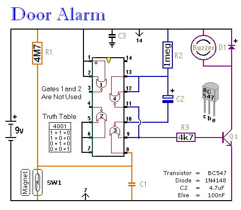
This is a straightforward and easy-to-assemble multi-purpose alarm system. It can be constructed using stripboard or veroboard along with a few inexpensive, readily available components. The alarm is designed to be installed on doors, windows, sheds, garages, cupboards, and...
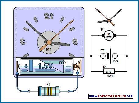
The circuit described is suitable for indicating the capacity of a battery using a low-cost electric clock. By connecting a resistor across the battery terminals, the battery discharges at a faster rate than it would with the clock alone....
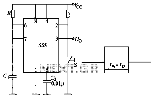
Introduction to the circuit schematic depicted in Figure 3-3. In this configuration, the 555 timer is utilized in a monostable mode, typically activated by a normally open push button switch. The circuit operates in an S-shaped state, where the...

The ongoing debate regarding the superiority of valves versus transistors is not the focus here. However, for those undecided, this simple amplifier serves as an excellent test. It employs a valve as a pre-amplifier and a MOSFET in the...
The loop antenna L1 is utilized for emission and also functions as the oscillation coil. The high-frequency current flowing through the antenna is synchronized in resonance with the oscillation frequency, ensuring optimal emission performance. Practical applications indicate that the...

This simple circuit is designed to detect RF radiation leakage from transmitters, faulty connections, broken cables, or equipment with inadequate RF shielding. It is specifically tailored for the 2-meter amateur radio band (144-146 MHz in Europe). The device features...