
Simple Pyro RF Transmitter (27 MHz) Circuit
")
The circuit schematic represents a compact design that efficiently integrates multiple functionalities within a limited space. The mixing of signals at the base of transistor T2 is a critical operation, as it allows for the modulation of the RF transmission signal. The careful selection of through-hole components is essential to maintain the integrity of the circuit while maximizing space utilization.
The ground plane is a vital component of the design, as it not only provides a common reference point for all components but also enhances the performance of the antenna. The thickness of the traces is a consideration in the design process, as it can influence the overall performance of the circuit, especially in RF applications. While smaller traces are typically recommended for higher frequency applications to reduce parasitic capacitance and inductance, the chosen width is adequate for the low-frequency operation of this circuit.
The layout also emphasizes the importance of the toner transfer method in PCB fabrication, where the reversed text is a common occurrence. This method requires careful attention to detail to ensure that the final product meets design specifications. The integration of additional features, such as the PyroElectro.com text, demonstrates the flexibility of the PCB design process and the ability to incorporate branding or identification into the layout without compromising functionality. Overall, the schematic effectively illustrates a well-thought-out design that balances complexity and simplicity in its execution.The schematic for this project is actually deceivingly simple compared to the complexity of what is happening in the circuit. So take a look below or click to view the full sized schematic. The two signals we`ve just generated are mixed together at the base of T2 and once it goes out of the collector of the transistor our continuous wave RF trans
mission signal is ready. The board layout was done in a way so that everything was crammed together very tight. This is a difficult thing to do with through-hole parts, but not impossible. A ground plan covers the entire board (but is chopped up by the traces) so that all parts that need access to ground can have it easily. The ground plan is also very important as its acts as part of our antenna. I just chose a nice thick width that would transfer over nicely when building the PCB, however smaller trace widths seem to be a better choice when designing RF circuits.
but at these low frequencies I don`t believe there will be any performance benefit. My PC board had extra space so I plugged in PyroElectro. com. You`ll notice the text is backwards, this is because during the toner transfer process, a bottom layer is technically printed out backwards, but once on the PCB it reads correctly. 🔗 External reference
Related Circuits
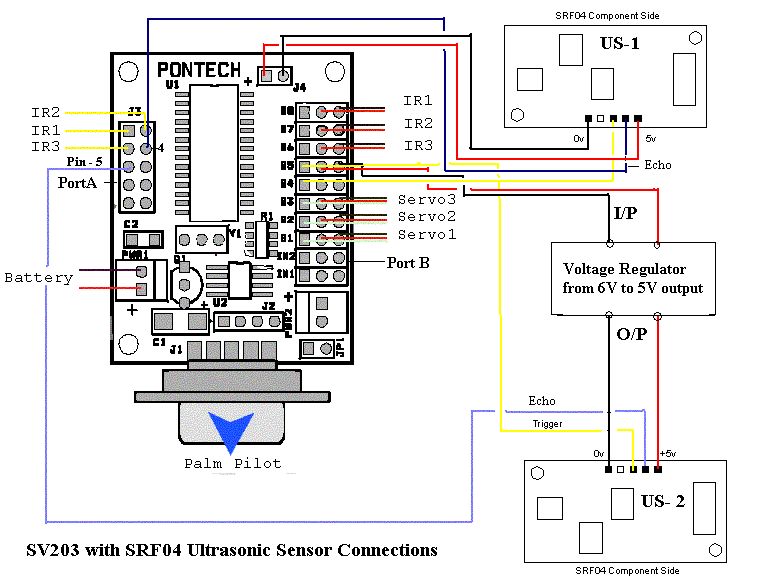
The following circuit illustrates the connection of the Devantech SRF04 Ultrasonic Sensor to the SV203 powered PPRK Circuit Diagram. This circuit is based on the Devantech SRF04 sensor and features a minimum initiation time of 10 milliseconds for the...

Any type of flashing light on the main brake lights is prohibited and illegal in most states of the U.S.A. Verification is being conducted for the same in Canada. Meanwhile, using this circuit is at one's own risk, with...

One LTC 1149 synchronous switching regulator can deliver both 3.3 and 5 V outputs. The design's simplicity, low cost, and high efficiency make it a strong contender for portable, battery-powered applications. The circuit described accepts input voltages from 8...
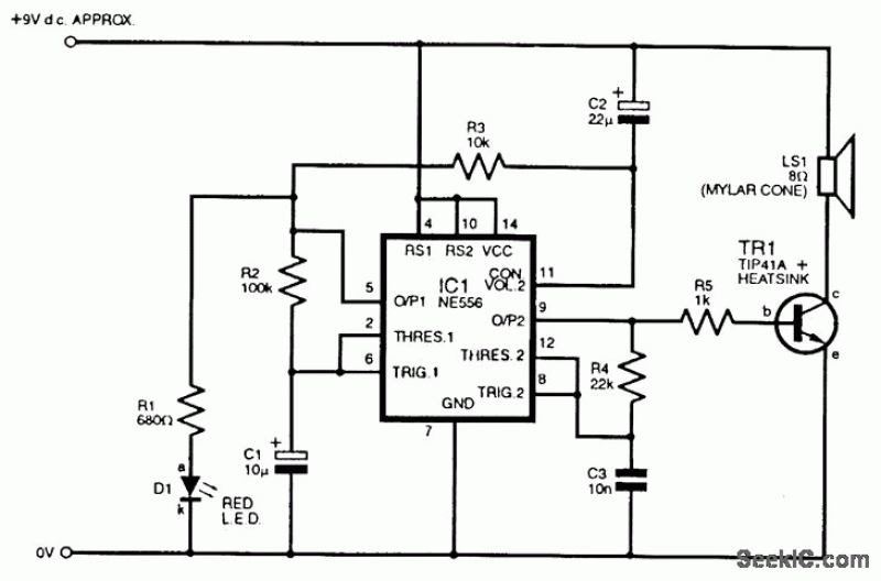
An adaptable siren generator circuit with multiple applications is presented. It is based on a 556 twin-timer chip, IC1. One timer section generates an audio tone that is directly coupled to the driver transistor, TR1. The other half of...

The schematic for the board is illustrated below. The three primary components of the board include (1) the power input and voltage regulation, (2) the L297 input and outputs, and (3) the L298 stepper motor control circuit. The motor...

The circuit utilizes a motor auto-voltage transformer for starting. The motor auto-voltage transformer start circuit is designed to provide a controlled method for initiating the operation of an electric motor. This type of circuit is particularly beneficial in applications where...