
Simple structure hi-fi amplifier

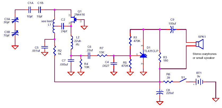
The circuit described utilizes a minimalist approach with four transistors, which are strategically arranged to achieve a high-fidelity amplification of the input signal. The PNP transistor (VT1) at the input stage is crucial for matching the input impedance, ensuring that the circuit can effectively interface with various signal sources without significant signal loss or distortion. The voltage amplification stage, facilitated by VT2, is configured in a common emitter mode, which is well-known for providing substantial voltage gain while also inverting the phase of the input signal.
Transistors VT3 and VT4 form a complementary push-pull output stage, which is essential for driving loads efficiently. This configuration allows for improved linearity and reduced distortion in the output signal, making it suitable for high-quality audio applications. The negative feedback loop, established through resistors R7 and R, plays a vital role in stabilizing the gain of the amplifier. The gain equation provided indicates that the circuit can be fine-tuned by adjusting the values of R7 and R, thereby allowing for versatility in various applications.
The bootstrap capacitor C3 enhances the amplifier's performance by improving the frequency response and stability, particularly at higher frequencies. Additionally, the isolation resistor R6 helps to prevent unwanted interactions between different stages of the circuit, ensuring that each transistor operates within its optimal range. Overall, this circuit design exemplifies a well-engineered amplifier capable of delivering high-fidelity audio output with minimal distortion, making it suitable for demanding audio applications. Circuit shown in Figure 240 of the circuit structure is very simple, with only four transistors to achieve circuit from input voltage put large, inverted, and promote the whole process of the amplifier, and a high technical indicators circuit, is an excellent high-fidelity power discharge path. VTi for the input stage, the use of a PNP transistor input stage and both impedance matching function, VTz voltage amplification stage and both CE and inverted push function, VT3 and VT4 constitute complementary push-pull amplifier output stage O R7, and R Pat negative feedback loop and determine the circuit gain: Av-R7 cuddle 8-2.7/0.22, together 21dBo bootstrap capacitor C3, R6 for the isolation resistance.
Related Circuits

This circuit can be directly connected to CD players, tuners, and tape recorders. It requires the addition of a 10K logarithmic potentiometer (dual gang for stereo) and a switch to accommodate various sources. Proper grounding is crucial to eliminate...
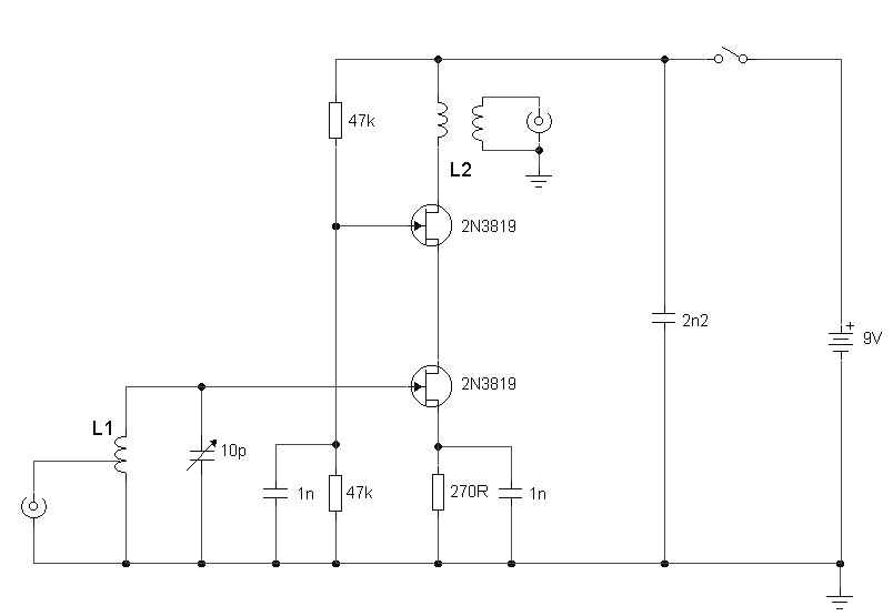
The circuit design utilizes a VHF amplifier configured to operate within the frequency range of 88 to 108 MHz, specifically for Band 2 radio applications. The VHF amplifier circuit is designed to enhance weak radio frequency signals in the specified...
A brief background is provided, indicating a basic understanding of electronics, including knowledge of component functions and schematic reading, but lacking further expertise. The circuit in question appears to involve fundamental electronic components, which may include resistors, capacitors, diodes, transistors,...
The circuit diagram represents a simple yet effective intercom system entirely based on transistors. It consists of three stages along with an RC amplifier. When the pushbutton S2 is pressed, the amplifier circuit around transistor T1 is activated. The intercom...
Wind 6 turns of solid wire on a pen or pencil that is just under 1/2 inch in diameter. Remove the wire from the pencil and spread the winding to make a length of 3/4 inch. Solder C2 somewhere...
It is advantageous to adjust the gain of an amplifier circuit without modifying more than one resistor value, unlike the previous design of the differential amplifier. The instrumentation amplifier builds upon the last version of the differential amplifier to...