
Simple transistor tester circuits

The transistor tester is a crucial tool in electronic diagnostics, designed to evaluate the functionality of transistors and other semiconductor devices. It typically operates by applying a small voltage to the transistor's terminals to determine its operational state. The tester can identify whether the transistor is functioning properly, whether it is open or shorted, and can also measure key parameters such as current gain (hFE), base-emitter threshold voltage, and collector-emitter breakdown voltage.
In a typical schematic, the transistor tester circuit may consist of a microcontroller or an operational amplifier that processes the signals from the transistor under test. The circuit often includes a display unit, such as an LCD or LED indicators, which provides real-time feedback on the test results. Additionally, resistors and capacitors may be incorporated to stabilize the circuit and filter out noise, ensuring accurate measurements.
The design of the PCB for the transistor tester should facilitate easy connections to the transistor leads, often through dedicated test probes or sockets. Proper layout considerations must be taken into account to minimize parasitic capacitance and inductance, which can affect the accuracy of the measurements. Power supply requirements should also be addressed, with provisions for both battery and external power options.
Overall, the integration of a transistor tester into a circuit or PCB enhances troubleshooting capabilities, allowing engineers and technicians to quickly assess the health of transistors and ensure the reliability of electronic systems.This is the Transistor tester into the Circuit or PCB. When your project do not works, the tester electronic parts or.. 🔗 External reference
Related Circuits
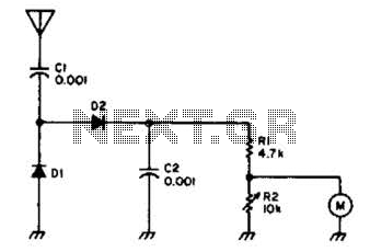
Useful for checking transmitters and antennas, this circuit utilizes a voltage-doubling detector consisting of diodes D1 and D2, which can be HP 5082-2800 hot carrier types or alternatives such as 1N34 or IN82. The circuit incorporates a 100-mA meter...
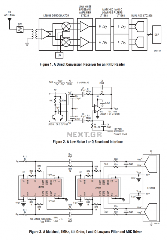
Figure 1 shows the block diagram of a direct conversion RF receiver—the receiver demodulates an RF carrier directly into a baseband signal without an intermediate frequency down-conversion (a zero IF receiver). The antenna, shared by both the transmitter and...
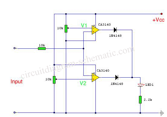
This circuit diagram indicates when the input voltage deviates from two defined limits, V1 and V2. The limits are adjustable, and the circuit is designed to trigger the adjustable window. The supply voltage, Vcc, must be at least 2...
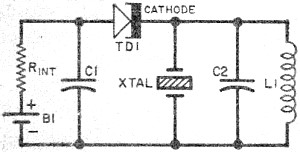
Leo Esaki invented the tunnel diode in 1957 while working at Sony (then known as Tokyo Tsushin Kogyo). Tunnel diodes feature a very narrow, heavily doped p-n junction approximately 10 nm wide, which exhibits a broken bandgap. This configuration...

The initial section of the circuit is a preamplifier that utilizes transistor Q1 (2N2222). The collector of transistor Q3 is connected to the base of transistor Q2 (2N2905A), which creates a complementary symmetry pair with Q3 (2N3053). The amplified...

This simple filter utilizes an RC section as the filter element, incorporating a voltage follower to manage other frequencies. The -3 dB point is calculated as 1/(6.28 * RXCV), resulting in a response that drops 6 dB per octave...