
Sine Signal Generating

Changing the device`s parameters is OK. (View) Burr-Brown 4302 multifunction converter and opamp generate hyperbolic sine transfer function with response matching ideal curve within 0. 7%. Technique permits setting powers and roots at fractional as well as integer values. Converter shown is set for exponent of 3. 2. Choice of amplifier gain and ref erence voltage scales response for given input and output signal levels. Article gives design equations. -J. Graeme, Sinh Generator Boasts 0. 7% Error, END Magazine, Aug. 5, 1978, p 70 and 72. (View) Opamp is used as tuned circuit driven by square wave from yoltage comparator Frequeny is controlled by R1-R3, C1, and C2, with R3 providing tuning.
Comparator is fed with resulting sine wave to obtain square wave for feedback to input of tuned circuit, to cause oscillation. Zener stabifizes amplitude of square wave that is fed back. R6 and C5 provide DC negative feedback around com arator to ensure starting. Values of C1 and C2 are equal, and range from 0. 4 F for 18 80Hz to 0. 002 F for 4. 4-20 kHz. ``Easily Tuned Sine Wave Oscillator, ³National Semiconducotor, Santa Clara, CA, 1971, LB-16. (View) Uses National SK0003 sine/cosine look-up table kit consisting of four MOS ROMs and three output adders.
Combination implements equation sin =sin M cos L + cos M sin L. Worst-case error is 1 5/8 bits in least significant bit. Cosine is approximated with loss in resolution of1/2 bit in 11-bit input or1/4 bit in 10-bit input. - Memory Databook, National Semiconductor, Santa Clara, CA, 1977, p 6-98-6-99. (View) Combination of SN72310 voltage-follower opamp and SN 72301A high-performance opamp gives two outputs differing in phase by 900. Supply is ±18 V. - The Linear and Interface Circuits Data Book for Design Engineers, Texas Instruments, Dallas, TX, 1973, p 4-40.
(View) Uses NE571 analog compandor in oscillator circuit based on Wien network formed by R1-C1 and R2-C2, placed around output amplifier of section A to make it bandpass amplifier. Section B serves as inverting amplifier with nominal gain of 2. Total harmonic distortion is below 0. 1%. Operating frequency is about 1. 6 kHz for values shown, but can be varied from 10 Hz to 10 kHz. Frequency is l/21 RCforR = R1 = R2 and C = Cl = C2. R should be kept between 10K and 1 megohm and C between 1000 pF and 1 F. Useful as fixed-frequency oscillator but can be tuned if matched dual pot is used for R1. R2. -W. G. Jung, Gain Control IC for Audio Signal Processing. Ham Radio, July 1977, p 47-S3. (View) Squarewave oscillator Q2-Q3 stabilized by Q1, followed by passive filter and active filter using A709, produces amplitude-stabilized sine wave at 350 Hz, for which third harmonic is 39 dB down and other harmonics are insignificant.
-E. Neugroschel and A. Paterson, Amplitude-Stabilized Audio Oscillator, EEE Magazine, April 1971, p 65. (View) Output voltage is 8 V P-P at about 25 Hz for values shown, with total harmonic distortion less than 0. 5%. Circuit will operate from 15 Hz to 100 kHz by using other values. Set regeneration control Rl, at minimum value needed to sustain oscillation. -J. C. Freebom, Simple Sinewave Oscillator, EDN/EEE Magazine, Sept. 1, 1971, p44. (View) Peak detector is used with FET operated in voltage variable. -resistance mode. in combination with standard double-integration circuit having regenerative feedback. to give 1. 46-kHz sinewave output into 500-ohm load at 10 V P-P. Will operate at power supply voltages off 8 to 18 V whhout appreciable variation in output amplitude or frequency.
Output varies less than 1. 5% in frequency and 6% in amplitude 🔗 External reference
Related Circuits
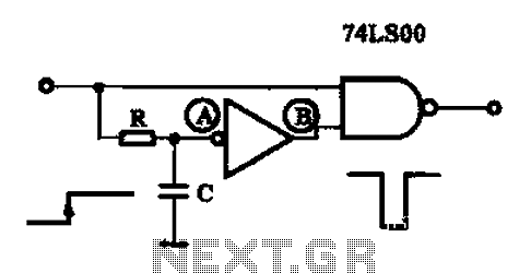
A single pulse signal generating circuit is designed to produce a one-shot pulse output. This circuit can be utilized in applications requiring a digital reset signal or to halt a signal. It operates as a non-synchronous differential circuit. The single...
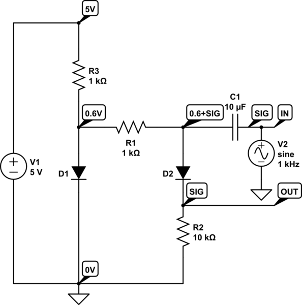
D1 compensates for the forward voltage drop of D2 by providing a 0.6V bias. The +5V is an external source. D1, R1, and R3 create a 0.6V bias on the capacitor's other side, allowing a positive signal swing to...

Amplify a MG811 CO2 sensor to a range readable by an ATMEGA2560 (0-5V). Other analog sensors are in use, so it is preferred not to change the reference voltage on the ATmega. A module that scales the signal has...
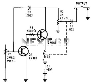
Useful for troubleshooting audio, video, and lower frequency RF amplifiers. This circuit generates a signal that is rich in harmonics. The circuit designed for troubleshooting audio, video, and lower frequency RF amplifiers is crucial for diagnosing issues in these systems....
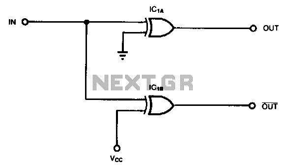
Some applications, such as driving three-state buffers for data multiplexers or for biphase clocks in high-speed systems, require complementary signals with minimal time skew and nearly simultaneous transitions. In this context, XOR gates serve as both inverting and non-inverting...
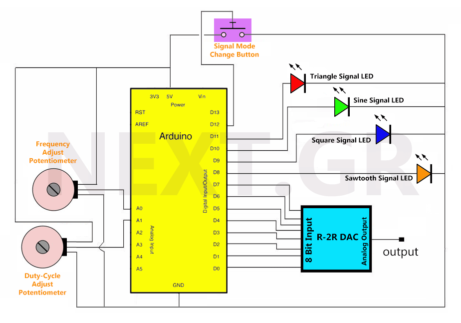
Once the circuit receives power, all variables are initialized, and the loop function runs continuously. Initially, all LEDs are off, and there is no output signal. Pressing the signal switch activates the first LED, indicating the output signal. The...