
A single pulse signal generating circuit

The single pulse signal generating circuit, commonly referred to as a one-shot pulse generator, is essential in various electronic applications where precise timing and control of signal pulses are required. This circuit typically employs a combination of resistors, capacitors, and active components such as operational amplifiers or timers (e.g., 555 timer IC) to achieve its function.
In operation, the circuit is triggered by a specific input signal, which initiates the generation of a single output pulse of predetermined duration. The pulse width can be adjusted by modifying the resistor and capacitor values in the timing network, allowing for flexibility in different applications. The non-synchronous aspect of this circuit means that it does not rely on a clock signal for operation; instead, it responds directly to the input trigger.
The output pulse can be used in various scenarios, such as resetting digital counters, generating clock signals for sequential logic circuits, or controlling the timing of other electronic devices. Additionally, the circuit can include features such as output buffering to drive larger loads or integration with microcontroller systems for enhanced control and functionality.
Overall, the single pulse signal generating circuit is a versatile tool in digital electronics, providing reliable and precise pulse generation for a wide range of applications.A single pulse signal generating circuit Shown as a single pulse signal generating circuit, switch contacts such as the use of such a digital signal reset signal or the stop si gnal is to be formed, this one-shot pulse generating circuit can be used. This circuit is a non-synchronous differential circuit.
Related Circuits
Unfortunately, there is no breadboard available for testing; however, modifications can be made to the PCB. The 1K potentiometer has been removed until the strobe functionality can be established. The circuit in question appears to involve a strobe light mechanism,...
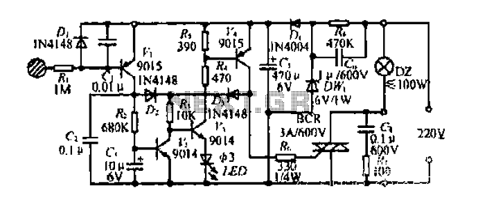
Diagram 2 depicts a shake tube circuit with a capacitance (C) and a trigger voltage rectifier filter element. The circuit includes a trigger voltage transistor amplifier (H), three pull tubes (n, U, v), and utilizes a thyristor as a...
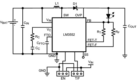
For this LED driver electronic project, a DC power supply circuit is required to provide an output voltage between 2.7V and 5.5V. The supply voltage must be applied between Vin and GND. The T/F jumper connects the T post...
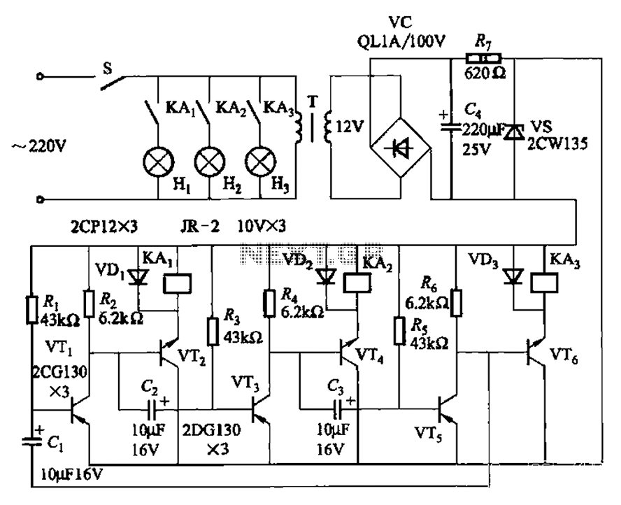
The transistors VTi, VT3, and VTs, along with the RC components, form three distinct multi-resonator oscillators. The oscillation frequency levels are dependent on the values of Ri, R3, Rs, and Cl, as well as Cz and C3s. The circuit comprises...
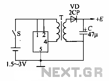
A DC booster circuit is illustrated in the figure, which represents a step-up transformer circuit diagram. The step-up transformer (T) can be utilized to power small transistor radios. The winding ratio can be adjusted to achieve the desired output...
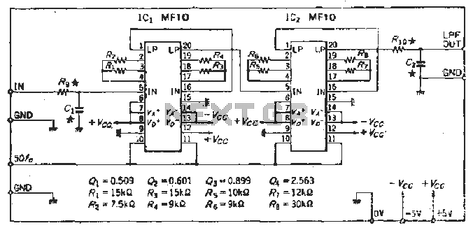
To create a Butterworth low-pass filter with a 12 dB/octave roll-off, four second-order (12 dB/oct) filter blocks are connected in series. This configuration is intended to achieve flat response characteristics across the frequency spectrum. The values for each stage...