
Solid laser range finder reception circuit

This circuit exemplifies a high-gain amplifier designed for applications requiring significant signal amplification with a wide bandwidth. The gain of 12,000 indicates that the circuit is suitable for low-signal applications, where even minute input signals can be amplified to usable levels. The specified bandwidth of 0.5 to 14 MHz suggests that the circuit can handle a variety of signal frequencies, making it versatile for different electronic applications.
The input resistance of 700 ohms is relatively high, allowing for minimal loading on the preceding stage, which is crucial in maintaining signal integrity. Conversely, the output resistance of 35 ohms, measured at 5 MHz, indicates a low output impedance, which is beneficial for driving subsequent stages or loads without significant loss of signal strength.
The direct coupling configuration of transistors T1 and T2 allows for efficient signal transfer between stages without the need for coupling capacitors, which can introduce phase shifts and frequency response issues. The parallel current negative feedback employed in this design stabilizes the gain and improves linearity, thus reducing distortion and enhancing overall performance.
The inclusion of the Zener diode 2CW11 serves a critical role in regulating the emitter voltage of transistor T2, ensuring that the transistor operates within its optimal range. This regulation helps to maintain consistent performance across varying operating conditions and contributes to the stability of the amplifier.
Overall, this circuit design is well-suited for applications in audio amplification, RF signal processing, and other areas where high gain and low noise are essential.The amplification of this circuit is about 12000 times, the bandwidth is 0.5~14MHz, the input resistance is 700?, the output resistance is 35?(measured with 5MHz), the output noise level is 0.6~0.8V. In figure, T1, T2 are direct coupling amplifier, they are connected into parallel current negative feedback.
Zener diode 2CW11 improves T2 emitter level, i.. 🔗 External reference
Related Circuits
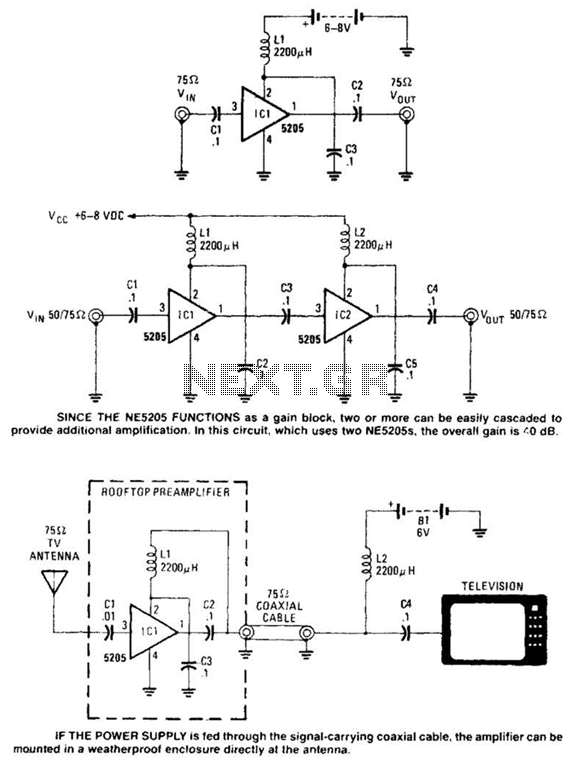
Except for the coupling and decoupling capacitors, IC1 is a complete wideband amplifier that has a fixed gain of 20 dB up to 450 MHz. No external compensation is required. Since the NE5205 functions as a gain block, two...
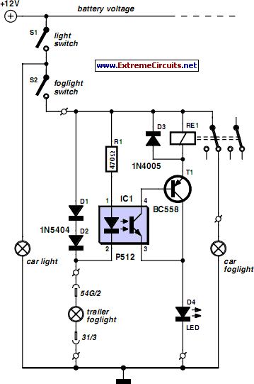
For several years, a rear fog lamp has been mandatory for trailers and caravans to enhance visibility in foggy conditions. When the fog lamp is activated, the fog lamp of the towing vehicle must be turned off to prevent...

The DW10M de-excitation type switch is based on the DW10 automatic air circuit breaker, transitioning from normally open to normally closed contact. The models available include DW10M-200, DW10M-400, and DW10M-600. The control circuit for this type switch is illustrated...
The gate-source voltage required to bias the transistor into the linear region can range from 0.25V to 8V, resulting in a potential variation of 7.75V down to a minimal 0.4V for the transistor and load when used with a...
Long-range FM transmitter. The power output of most of these circuits is very low because no power amplifier stages were incorporated. The transmitter circuit described here has an. The long-range FM transmitter operates by modulating a carrier frequency with an...
This document presents a collection of compact, self-contained alarm circuits. These circuits are designed to operate with a very low standby current, making them ideal for battery-powered applications. They can be triggered by both normally-open and normally-closed switches, while...