
STEREO TV DECODER

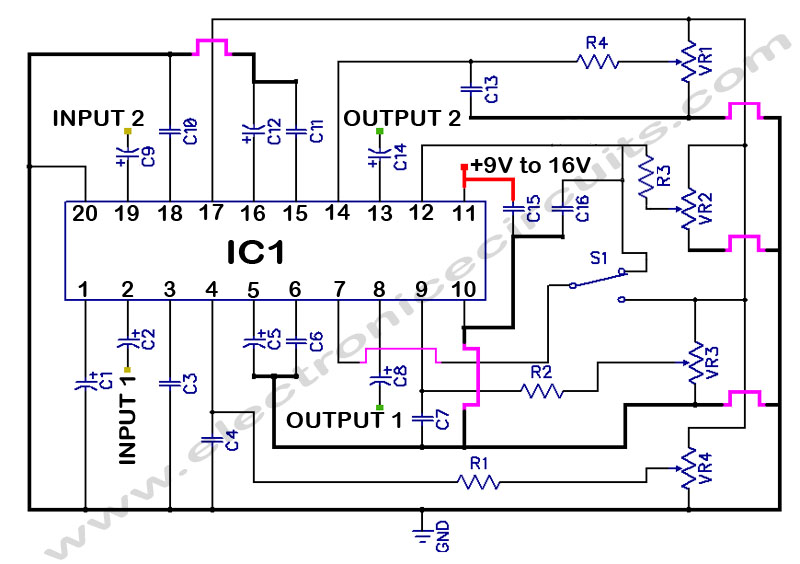
The stereo TV decoder circuit is designed to effectively demodulate and process audio signals for stereo television reception. The core component, IC1, operates at a frequency of 4.5 MHz, which is optimal for audio demodulation in stereo systems. The switch connected to IC1 allows the user to select between different demodulation sources, which adds versatility to the circuit.
IC2-a serves as a buffer amplifier, ensuring that the signal integrity is maintained when interfacing with the LM1800 stereo demodulator (IC3). This demodulator is critical for extracting the left and right audio channels from the incoming signal. The outputs from IC3 are designed to provide discrete audio channels, which are essential for stereo sound reproduction.
The use of op-amp IC4-a as a difference amplifier is a key design choice, as it effectively regenerates the L-R signal by combining the left and right channel outputs. The integration of capacitor C18 plays a dual role; while it slightly reduces the high-frequency separation, it simultaneously minimizes distortion, thus enhancing the overall audio quality.
The subsequent filtering stages, including the 12 kHz low-pass filters, ensure that both the L+R and L-R signals are phase-aligned, which is essential for maintaining audio fidelity. The inclusion of Q2 allows for level control, which is important for balancing the audio output, and its inverting function compensates for previous signal inversions.
The expander stage, utilizing the NE570, is designed to restore the dynamic range of the audio signal by mitigating low-frequency noise and ensuring that the final output is clean and free from unwanted artifacts. The design of the high-pass filters at various stages of the circuit is crucial for preventing low-frequency noise from affecting the audio output, thereby enhancing the listening experience.
Overall, the stereo TV decoder circuit is a well-structured design that combines various components and techniques to achieve high-quality audio demodulation and processing, ensuring that users receive a superior stereo sound experience.A block diagram of the stereo-TV decoder is shown in A. It shows the overall relationships be-tween the separate sections of the circuit; B through E show the details of each subsection. The de-coder section centers around IC1, a standard 4. 5-MHz audio demodulator. The output of IC1 is routed to 51, which allows you to choose between the internall
y demodulated signal and an exter-nally demodulated one. Buffer amplifier IC2-a then provides a low-impedance source to drive IC3, an LM1800 stereo demodulator. When IC3 is locked on a stereo signal, the outputs presented at pins 4 and 5 are discrete left- and right-channel signals, respectively.
In order to provide noise reduction to the L-R signal, you must recombine the discrete outputs into sum and difference signals. Op amp IC4-a is used to regenerate the L-R signal. It is wired as a difference amplifier, wherein the inputs are summed together (+L -, R). Capacitor C18 bridges the left- and right-channel outputs of the demodulator. Although it decreases high-frequency separation slightly, it also reduces high-frequency distortion. The L + R signal is taken from the LM1800 at pin 2, where it appears at the output of an internal buffer amplifier.
The rawL -R signal is applied to IC4-b, a 12-kHz lowpass filter. The L + R signal is also fed through a 12-kHz low pass filter in order to keep the phase shift undergone by both signals equal. Next, the L - R signal is fed to Q2. It allows you to add a level control to the L - R signal path; it provides a low source impedance for driving the following circuits, and it inverts the signal 180 °.
In-version is necessary to compensate for the 180 °inversion in the compander. Next comes the expander stage. At the collector of Q2 is a 75- s de-emphasis network (R27 and C29) that functions just like the network that is associated with Q1. Note that Q2 feeds both Q3 and IC5-a, a -12-dB per octave high-pass filter. The output of that filter drives the rectifier input of IC6, an NE570. The 75-Hz high-pass filter at the rectifier input helps to prevent hum, 60-Hz sych buzz, and other low-frequency noise in the L - R signal from causing pumping or breathing.
The NE570 contains an on-board op amp; its irtverting input is available directly at pin 5 and via a 20-kO series resistor at pin 6. The 18-kQ resistor (R30) combines with the internal resistor and C32 (0. 01 F) to form a first-order filter with a 390- s time constant. Because the internal op amp oper-ates in the inverting mode, the -(L - R) signal is restored to the proper (L - R) form.
The output of the expander drives another 75-Hz high-pass filter, but this one is a third-order type that provides -18 dB per octave rolloff. It is used to keep low-frequency noise from showing up at the output of the decoder. At this point, the (L - R) signal has been restored, more or less, to the condition it was in before it was dBx companded at the transmitter.
🔗 External reference
Related Circuits
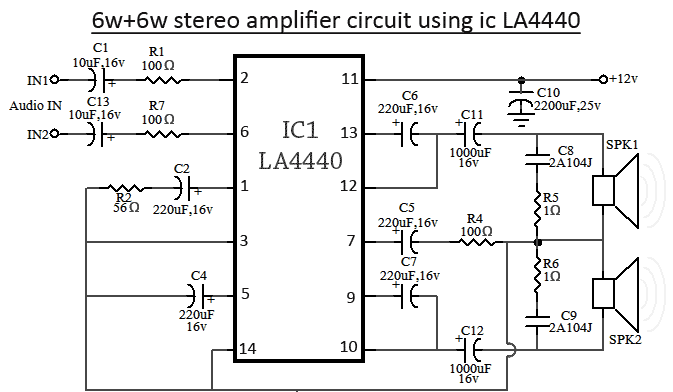
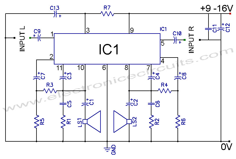
The LA4440 is a dual-channel audio amplifier integrated circuit (IC) that operates in two modes: stereo amplifier mode and bridge amplifier mode. This monolithic linear IC is produced by Sanyo. The circuit includes both amplifier modes utilizing the LA4440....
TDA2004 Car Battery 12W Stereo Amplifier Circuit. Its main features are low distortion, low noise, and high reliability of the chip. The TDA2004 is a highly integrated audio amplifier designed specifically for automotive applications. This circuit is capable of delivering...
The AD322 is an 8 amp G-Scale DCC decoder. The notes below may be beneficial to owners who wish to understand or repurpose ("hack") the decoder. It has a comprehensive set of functions that could easily be repurposed for...
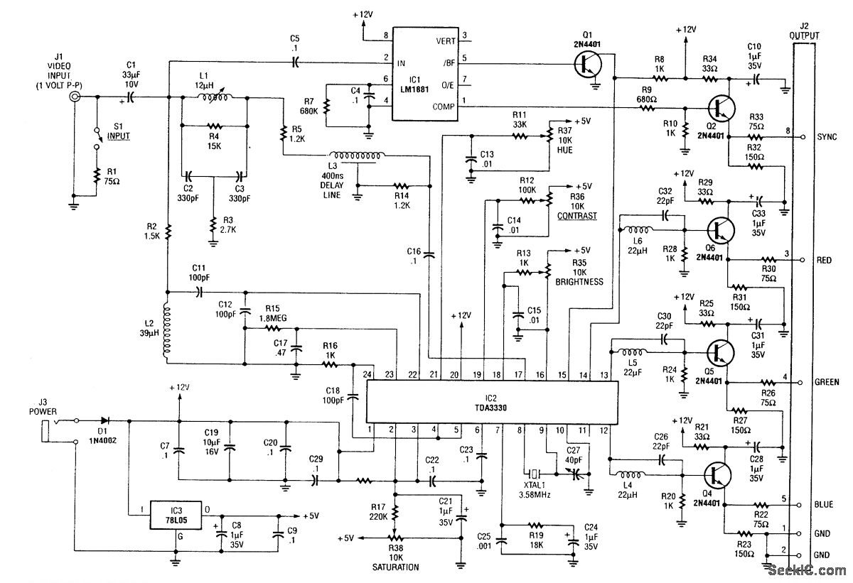
An NTSC/RGB decoder is presented, utilizing a TDA3330 to decompose a 1-V input video signal into its red, green, and blue components, as well as composite sync. The circuit includes an integrated sync separator (LM1881) designated as U1. This...
LM1036 Stereo Tone (Bass, Treble, Volume, Loudness, Balance) Controller Circuit. The LM1036 is a DC controlled tone (bass/treble), volume, and loudness controller designed for audio applications. The LM1036 circuit serves as an integrated solution for controlling various aspects of audio...
The BA5417 is a stereo amplifier integrated circuit (IC) that features several advantageous characteristics, including thermal shutdown, a standby function, soft clipping, and a wide operating voltage range. It can deliver 5 watts per channel into 4-ohm loudspeakers when...