
Suppress Jitter With Hysteresis Circuit

In this circuit design, a comparator is employed to monitor a specific voltage level and output a signal based on that level. The key components include resistors, capacitors, and transistors that work together to create a stable output with controlled timing characteristics.
The operation begins when the comparator detects a voltage level below a predefined threshold, resulting in a low output state. Upon the voltage rising above this threshold, the output transitions to high. This transition is coupled with a differentiation process through the capacitor Cl and resistor Rl, generating a sharp rising edge. This edge is critical as it triggers transistor Ql to turn on, effectively blocking the comparator's feedback through its strobing input. This action maintains the output in a high state for a period determined by the time constant formed by Rl and Cv, ensuring that the comparator does not react immediately to noise or fluctuations in the input signal.
Once the capacitor CI is charged by the current flowing through resistor R1, the voltage across CI reaches a level that turns off transistor Ql, thereby releasing the comparator to respond to further changes in the input signal. The process is mirrored when the output transitions from high to low, with the additional components R2, C2, and transistor Q2 managing the timing for this transition.
In applications where only one directional output transition is necessary, the circuit can be simplified by omitting the elements that provide temporal hysteresis for the opposite transition. This design choice enhances circuit efficiency and reduces component count, making it suitable for specific applications where rapid response to a single transition is critical. The overall design ensures reliable operation in various electronic systems, maintaining stability and responsiveness to input changes. When the comparator`s output changes its state from low to high, the rising edge of the output pulse, differentiated by the Cl/Rl chain, opens Ql. This blocks comparator via its strobing input and sustains its output in the state for a period of time, defined by the time constant RlCv After CI is charged by the current flowing through R1, Ql is shut off and the comparator is released.
When the comparator`s output state changes from high to low, a similar process, involving elements R2, C2, and Q2, occurs. In many applications, the output transition in only one direction is of vital importance, and the elements, which provide temporal hysteresis for the opposite direction transition, can be omitted.
Related Circuits
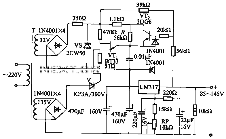
It utilizes a three-terminal adjustable voltage regulator power supply and incorporates a thyristor for presetting the LM317. The voltage can be adjusted between 85V and 145V, with an output current limited to a maximum of 1A. An adjustment potentiometer...
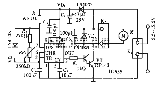
The circuit operates using pulse position modulation, which is a method distinct from the more commonly utilized pulse width modulation for speed control. A 555 timer is employed as a square wave modulator, generating output pulses with a fixed...
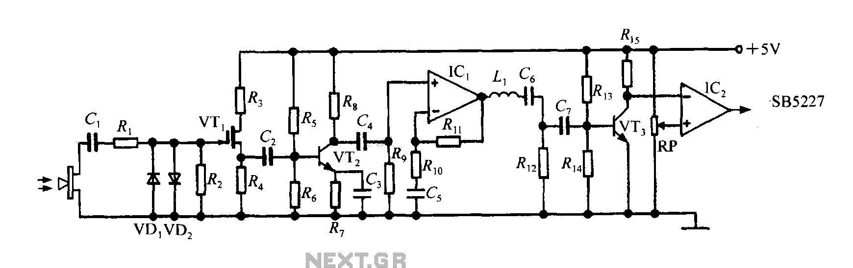
The SB5227 ultrasonic signal output is very weak and must be amplified via a power amplifier for effective transmission. A typical transmission circuit is illustrated in the accompanying figure. The SB5227 ultrasonic signal is sourced from output pin 10,...
The power supply terminal should utilize a 1 µF chip capacitor filter, positioned as close as possible to the chip's supply pin. The signal is generated by the input pins 2 and 3. The source resistance of the signal...
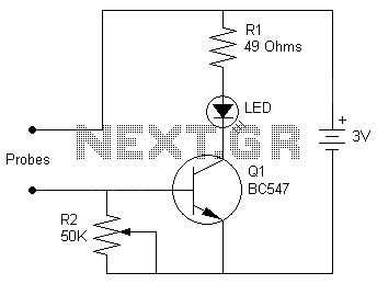
This project involves a straightforward soil moisture detection circuit that utilizes only four components and operates with a 3-volt battery. The circuit is designed to identify the presence of moisture in the soil of any plant and activate an...
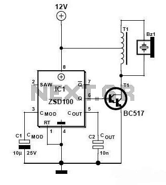
Zetex Semiconductors offers a siren driver integrated circuit (IC) known as the ZSD100, which is designed for use in alarm systems for vehicles and model crafts. By incorporating just a few additional components, as illustrated in the accompanying diagram,...