
Intelligent ultrasonic ranging ASIC SB5227 peripheral circuit design

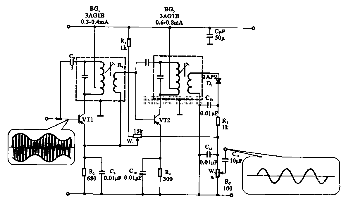
The SB5227 ultrasonic signal transmission and reception system is designed to optimize the performance of ultrasonic applications. The weak output signal from the SB5227 necessitates the use of a power amplifier to ensure sufficient transmission strength. The circuit begins with the ultrasonic signal generated at output pin 10, which is first buffered by a pair of amplifying transistors (VT1 and VT2). These transistors can either be low-power types or replaced with power FETs depending on the design requirements.
The receiver circuit is critically structured to enhance signal integrity and reliability. It starts with an input protection circuit comprising a DC blocking capacitor (C1), a current limiting resistor (R1), and two diodes (VD1 and VD2) which together form a bidirectional overvoltage protection mechanism. This ensures that the circuit remains safe from voltage spikes that could damage sensitive components.
Following this, the impedance matching and current amplification stage utilizes VT1, which is specifically selected as a J-FET to maximize performance. The voltage amplification stage involves VT2 and an operational amplifier (IC1, TL061), which provides additional gain to the received signal. The band-pass filter (L1, C6) is essential for isolating the desired frequency range, ensuring that the system is tuned to the same center frequency as the ultrasonic signal being transmitted.
The output-stage amplifier (VT3) further amplifies the filtered signal before it is processed by the voltage comparator (IC2, LM339). This comparator plays a crucial role in signal detection, toggling its output based on the presence of an ultrasonic burst. The system features an adjustment potentiometer (RP) that allows for fine-tuning of the receiver's sensitivity, enhancing its ability to reject noise and improve overall performance.
In terms of operational behavior, the circuit is designed to maintain a high output from IC2 during normal operation. When the first rising edge of the ultrasonic signal is detected, IC2's output transitions low, which signals the SB5227 to stop the internal timer at pin 8, effectively marking the start of the signal processing sequence.
To meet advanced technical requirements, the circuit may also be equipped with additional features such as automatic gain control (AGC) and an automatic search window circuit, which further enhance the system's responsiveness and adaptability in varying operational environments. Overall, this comprehensive design facilitates effective ultrasonic communication while ensuring robust signal processing capabilities.SB5227 ultrasonic signal output is very weak, it must be sent to the drive via the power amplifier. A typical transmission circuit as shown in FIG. SB5227 ultrasonic signal from the output pin 10, and a buffer amplifier F (VT1, VT2) drive transmitter. Using low-power transistors VT1, VT2 optional power FET. The receiver circuit includes the following six parts: input protection circuit (C1, R1, VD1 and VD2); impedance matching and current amplifier (VT1); two voltage amplifier (VT2, IC1); band-pass filter (L1, C6) ; output-stage amplifier (VT3); a voltage comparator (IC2).
C1 is a DC blocking capacitor, R1 is a current limiting resistor. VD1 and VD2 constitute bidirectional overvoltage limiter circuit. VT1 requires the use of J-FET, VT2 and VT3 selection of low-power transistors. IC1 is TL061 single op amp, IC2 is Quad voltage comparator LM339 (now only the way in which). Bandpass filter center frequency should be the same as the center frequency of the receiver. Adjustment potentiometer RP can change the receiver sensitivity, improve anti-jamming capability. Under normal IC2 output high, when receiving the first rising edge of the ultrasonic burst on output low, the SB5227 to the 8 feet, so that the internal timer is stopped counting. The technical conditions require a higher reception circuit, but also increase automatic gain control (AGC), automatic search window circuit.
Related Circuits
The demodulation and detection circuit is a radio AM intermediate frequency (IF) signal amplifier that performs two-stage detection using diode Dr. It extracts the audio signal from the IF carrier detection and subsequently sends it to the power amplifier...
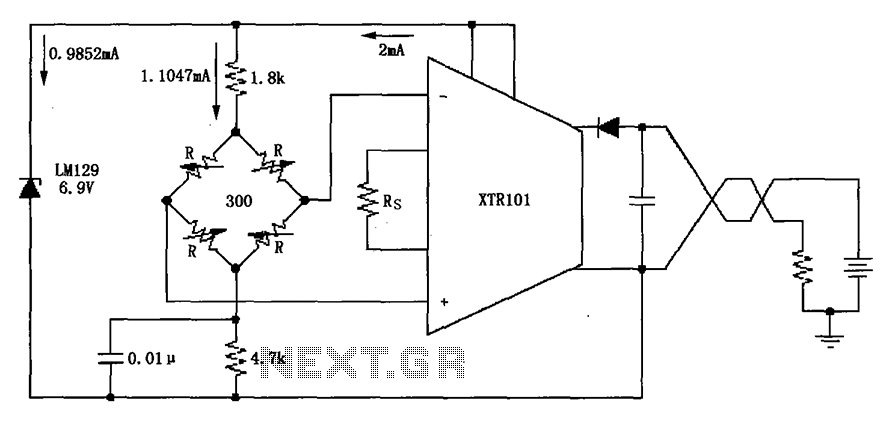
The circuit utilizes the LM129 voltage regulator to produce a 6.9V voltage reference, supplying a current of 1.0147mA from the 6.9V reference voltage to the bridge. The bridge may consist of varistor-type pressure sensors. The LM129 voltage regulator is a...
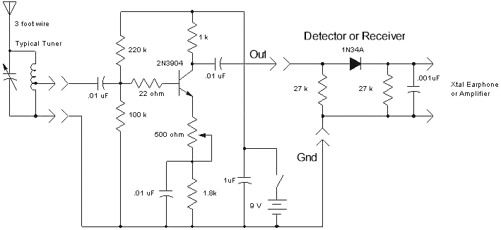
The crystal radio derives its name from the galena crystal (lead sulfide) utilized for rectifying signals. A "cat's whisker" wire contact was adjusted on the crystal's surface until a diode junction was established. The 1N34A germanium diode serves as...

Control a furnace using a 3.3V microcontroller. The furnace operates by connecting a common 21V AC "hot" line to one of two AC "neutral" output lines: Fan and Heat. When connected, they have relatively low current flow, approximately 100mA....
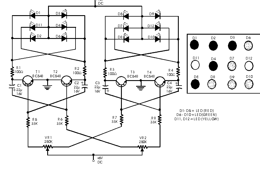
This circuit serves as a decorative element or indicator, featuring adjustable flashing or dancing speeds of LEDs and the ability to create various light patterns. It comprises two astable multivibrators; the first is constructed using transistors T1 and T2,...
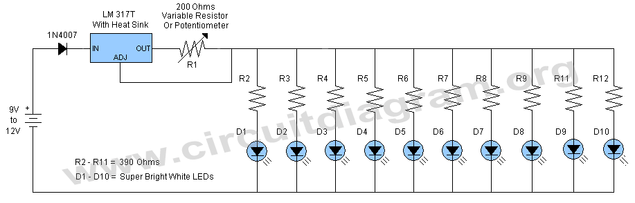
This schematic illustrates a simple yet effective LED dimmer circuit utilizing the well-known voltage regulator IC LM317T. The LM317T can function as a current regulator, as demonstrated in this circuit. It features ten super bright white LEDs, although the...