
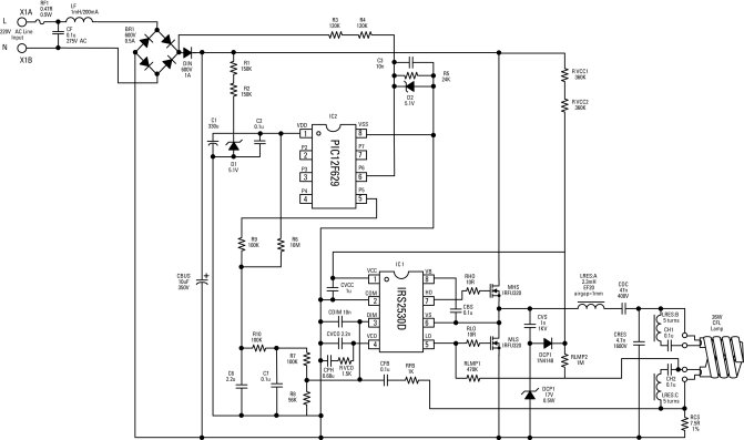
Switching power supply drive circuit

The driver circuit is integral to high-voltage applications where precise control of power switching is necessary. The variable width pulse width modulation (PWM) allows for fine-tuning of the output power, which is crucial in applications such as motor control, power supplies, and RF amplifiers. The isolation provided by the coupling transformer is essential for protecting the low-voltage control circuitry from high-voltage transients and noise that can occur during switching events.
The design of the drive transformer is critical; it must be optimized for low leakage inductance to ensure that the drive signals maintain their integrity and speed. The transformer should also be capable of handling the required current without saturating, which could lead to distortion in the output signal. Additionally, the choice of MOSFET driver is pivotal; it needs to be capable of delivering the necessary gate drive current quickly to minimize switching losses and ensure that the MOSFET operates efficiently.
In applications where electromagnetic interference (EMI) is a concern, the use of optocouplers can provide an additional layer of isolation while also helping to suppress noise. The shaping circuit preceding the transformer ensures that the output signal is clean and well-defined, which is vital for reliable operation of the MOSFET. The totem pole configuration allows for rapid switching by providing both sourcing and sinking capabilities, thus enabling fast transitions that are essential for high-frequency applications.
Overall, this driver circuit design exemplifies the integration of various electronic components to achieve a robust and efficient solution for controlling high-voltage power devices, ensuring performance reliability and safety in demanding operational environments.Driver circuit diagram: The main function of the driving circuit is variable width pulse width controller output power amplifier, as a drive signal to high voltage power switch ing device. Driving circuit generally have a role in isolation, often coupling transformer to achieve the high-voltage power switching devices incentive isolation between the input and output stages and, while both when the power switching device is turned off, reverse bias is applied, to accelerate the device on and off. When the drive MOSFET device, a conventional drive circuit is driven by a transformer to achieve. Taking into account the leakage inductance and lead inductance drive transformer to the main MOSFET having a large Cg-s high-speed charging and discharging cause difficulties, therefore, the usual way is to use a MOSFET driver drive transformer having a smaller Cg-S of the totem type driving circuit then this circuit driven by the main MOSFET.
As shown, the drive transformer primary input is the output signal of the drive signal control circuit, the output after shaping circuit shaping process after isolation transformer. Transformer isolators, optocouplers isolate both have anti-interference function, after shaping by Totem drive circuit drives the main MOSFET tube.
Related Circuits
Electronic ballasts for dimming fluorescent lamps require a control interface for the user to set the desired lamp brightness level. Existing interface circuits include a 1-to-10 Vdc interface, a digitally-addressable lighting interface (DALI), triac-based wall dimmers, three-way lamp sockets,...
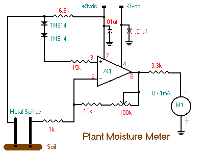
The following circuit illustrates a Plant Moisture Meter Circuit Diagram. This circuit is based on the LM741 integrated circuit (IC). Features include a meter that indicates moisture levels. The Plant Moisture Meter Circuit utilizes the LM741 operational amplifier to measure...

This constant gain, constant Q, variable frequency filter provides simultaneous low-pass, bandpass, and high-pass outputs. With the specified component values, the center frequency will be 235 Hz for high logic inputs and 23.5 Hz for low logic inputs. The...

This is a solid-state version of a Tesla coil, replacing the spark gap with MOSFET transistors and utilizing a close-coupled primary coil without capacitors. The method of driving the primary coil varies among designs. After researching various works online,...
This circuit functions as a motor controller, allowing for easy control and variation of the RPM and phase of an AC motor. The power source is directly 220VAC, and it can handle a load of approximately 1 horsepower AC...
This circuit performs a rapid battery test without requiring an external power supply or costly moving-coil voltmeters. It features two ranges: when switch SW1 is set as indicated in the circuit diagram, the device can test batteries ranging from...