
Tele Timer Circuit

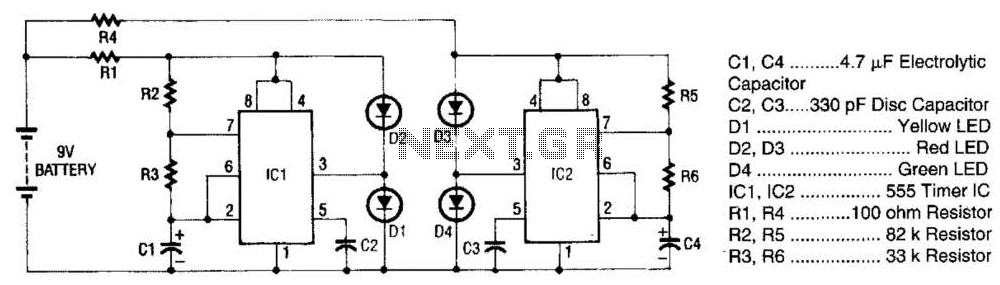
The circuit utilizes the 555 timer IC, a versatile device widely used for timing applications. The 555 timer operates in astable or monostable modes, and in this configuration, it primarily functions as a monostable timer. The long time period is achieved by adjusting the resistances in the timing network, which includes R3, R1, and R4, in conjunction with the timing capacitor C2. The charging and discharging of C2 dictate the duration of the output signal at pin 3.
When the circuit is powered, the initial state allows C2 to charge through the resistors and diode, creating a gradual increase in voltage across C2. The 555 timer's internal comparator monitors this voltage, and when it reaches a specific threshold (typically 2/3 of the supply voltage), it triggers the output to go low, thus discharging C2. The discharge path through R2 and D2 ensures that the timer resets and prepares for the next cycle. The activation of the piezo sounder during this phase creates an audible alert, which is a crucial feature for applications requiring notification.
For the short time period, the selection of R2 is critical. A 10 kΩ resistor will yield a short duration of approximately four seconds, while a 47 kΩ resistor extends this duration to around twenty seconds. This flexibility allows the circuit to be tailored to specific timing needs. The choice of capacitor C2 is also important; a low-leakage capacitor minimizes timing inaccuracies and ensures reliable operation over extended periods.
Overall, this circuit is a practical implementation of the 555 timer for dual timing applications, combining both adjustable and fixed timing periods with an audible output, making it suitable for various electronic projects and applications where timing and notification are essential. The circuit is built around a 555 oscillator/ timer. The circuit provides two time periods. The long-running time period is adjustable from about 1 to 10 minutes, and the short time period is preset to about three seconds. Here`s how the dual timer operates. When the power is switched on, G2 begins to charge through R3, Rl, Dl, and R4 to start the long-term timer period.
When the voltage across C2 reaches the 555`s internal switching point, the long-term timer times out, discharging C2 through R2, D2, and pin 7 of the 555. During that time, pin 3 of the 555 is pulled to ground, activating the piezo sounder. To set the short time period to about four seconds, use a 10 k resistor for R2, and for about twenty seconds use a 47 k resistor. The timing capacitor, C2, should be a good-quality, low-leakage unit.
Related Circuits
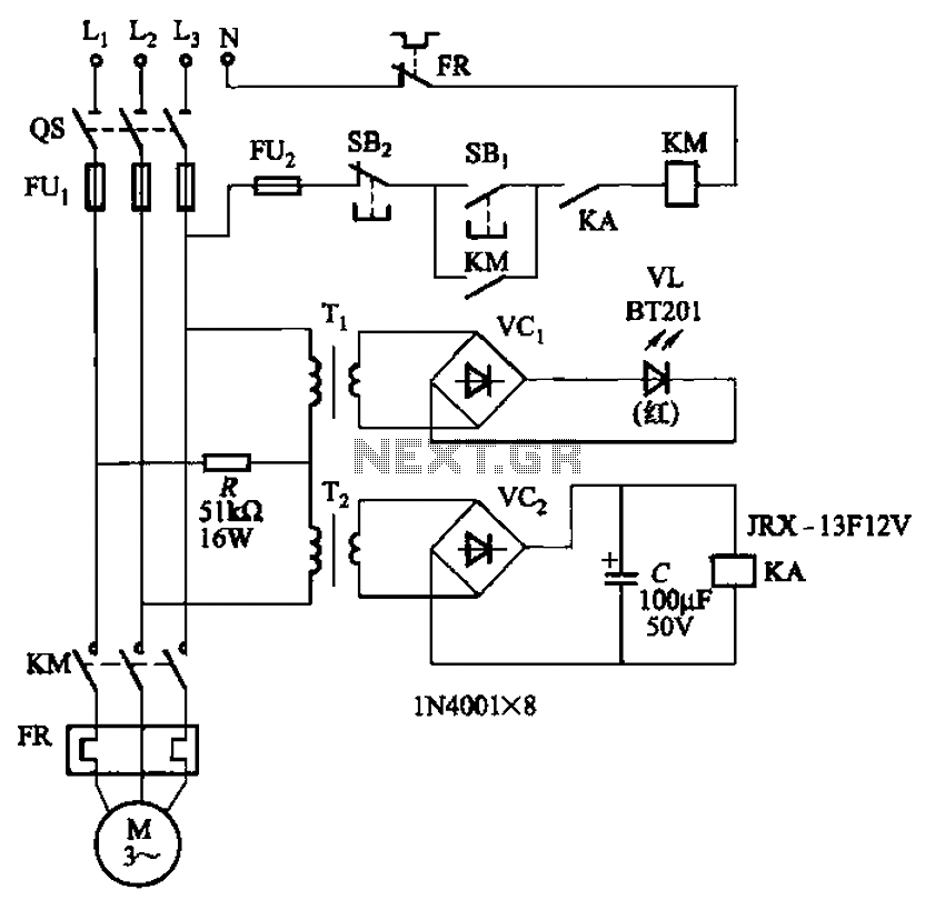
The circuit depicted in Figure 3-92 employs a dual-phase sequence protection relay for sensing. When the power supply exhibits a positive phase sequence (U, V, W), the relay KA is activated. If the power supply maintains the correct phase...
The super LED flasher consists of two complete LED flasher circuits integrated onto a single circuit board. The first LED flasher is comprised of IC1 and LEDs D1 and D2. IC1 is a 555 timer IC configured as an...
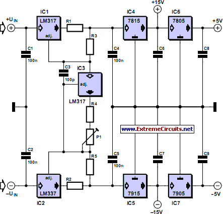
This current-limiting circuit, illustrated in this example as part of a small bench power supply, could theoretically be utilized alongside any dual-rail current source. The section of the circuit to the left of the diagram restricts the input current...
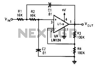
The circuit presented has a cutoff frequency of approximately 1 kHz. The resistors R1, R2, and capacitors C1, C2 can be adjusted to achieve any desired frequency. The circuit is designed as a filter, likely a low-pass or high-pass filter,...
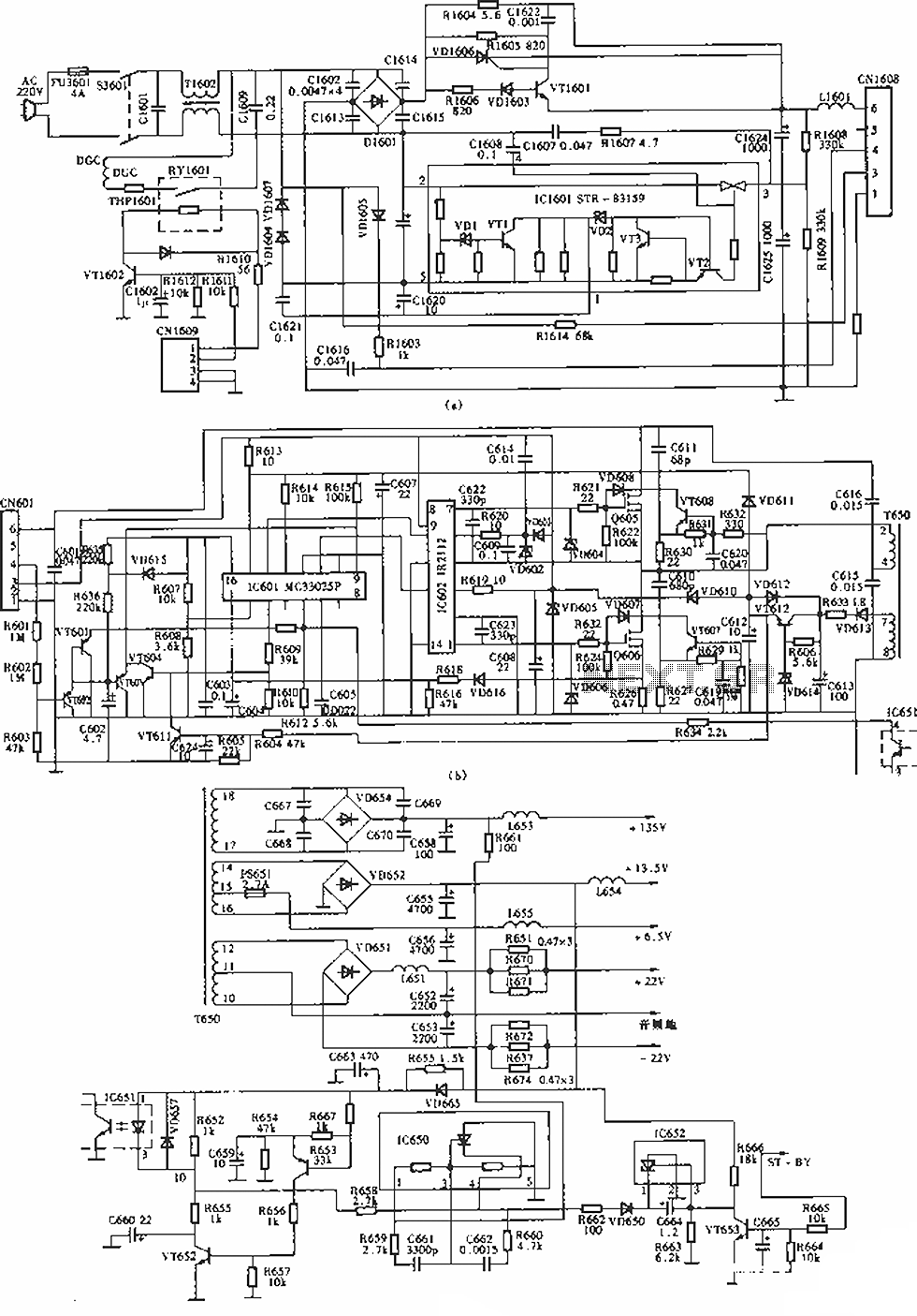
The circuit of the Sony KV-S29MHl (S Movement series) TV switching power supply (SIR a 80145A) consists of three main sections: (A) the power oscillation part, (B) the regulator part, and (C) the output section. The Sony KV-S29MHl TV switching...
The UC3842, UC3843, UC3844, and UC3845 series of oscillators can generate synchronization pulses without requiring numerous external components. The following circuit illustrates the Sync Pulse Generator Circuit Diagram for the UC3842/3/4/5. This sync pulse circuitry is capable of operating...