
Telephone Ring Generator Using Switching Supply

The telephone ring generator circuit operates by converting a low voltage input into a high voltage output suitable for ringing a telephone. The core of this circuit is a switching mode power supply (SMPS) that utilizes a CMOS Schmitt Trigger square wave oscillator. This oscillator generates a square wave signal that drives a high voltage switching transistor, such as the TIP47, which is capable of handling high voltage and current levels.
The design incorporates a 10 mH inductor, which is crucial for energy storage and transfer in the SMPS. The inductor must have a low DC resistance, ideally around 1.5 ohms, to ensure efficient operation and minimize power losses. The circuit also includes a driver transistor (2N3053) that amplifies the control signals to drive the high voltage transistor effectively.
To protect the circuit from excessive voltage, a 22K resistor is placed across the output. This resistor serves as a load, limiting the voltage to approximately 120 volts DC when the phone ringer is disconnected and around 90 volts DC when connected. The output voltage can be fine-tuned by adjusting a 150K resistor located between pins 10 and 11 of the oscillator circuit. This adjustment alters the frequency of the oscillator, which is typically around 800 Hz, a frequency suitable for telephone ringing.
The circuit is designed to produce a ringing signal for a duration of about 2 seconds, followed by a pause of approximately one minute between rings. This timing is controlled by a second Schmitt Trigger oscillator connected to pins 12 and 13. The timing intervals can be modified by changing the values of the 10K and 300K resistors connected to pin 12, allowing for customization of the ringing pattern based on user requirements.
In summary, this telephone ring generator circuit effectively combines various components and configurations to produce a reliable high voltage ringing signal, ensuring compatibility with standard telephone systems while allowing for adjustments in both output voltage and ringing duration.The telephone ring generator shown below generates the needed high voltage from a simple switching mode power supply (SMPS) which employs a CMOS Schmitt Trigger square wave oscillator, 10 mH inductor, high voltage switching transistor (TIP47 or other high voltage, 1 amp transistor) and a driver transistor (2N3053). The inductor should have a low DC resistance of 1.5 ohms or less. The switching supply must have a load connected to prevent the voltage from rising too high, so a 22K resistor is used across the output which limits the voltage to about 120 DC with the phone ringer disconnected and about 90 volts DC connected.
The output voltage can be adjusted by changing the value of the 150K resistor between pins 10 and 11 which will alter the oscillator frequency (frequency is around 800 Hz as shown). The supply is gated on and off by a second Schmitt Trigger oscillator (pins 12/13) so that the phone rings for about 2 seconds and then the circuit idles for about a minute between rings.
These times can be adjusted with the 10K and 300K resistors connected to pin 12. 🔗 External reference
Related Circuits

This schematic represents a radio receiver circuit based on the TDA7088T, which is suitable for use in mono portable and pocket radios. The TDA7088T is a bipolar integrated circuit designed to operate with a minimal number of peripheral components...
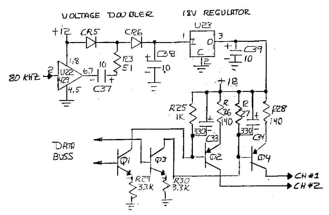
The DSC Sine and DRC Random vibration controller cards feature current sources on the two inputs that provide power to integrated accelerometers without the need for external power supplies. These current sources have an open circuit voltage of 18...
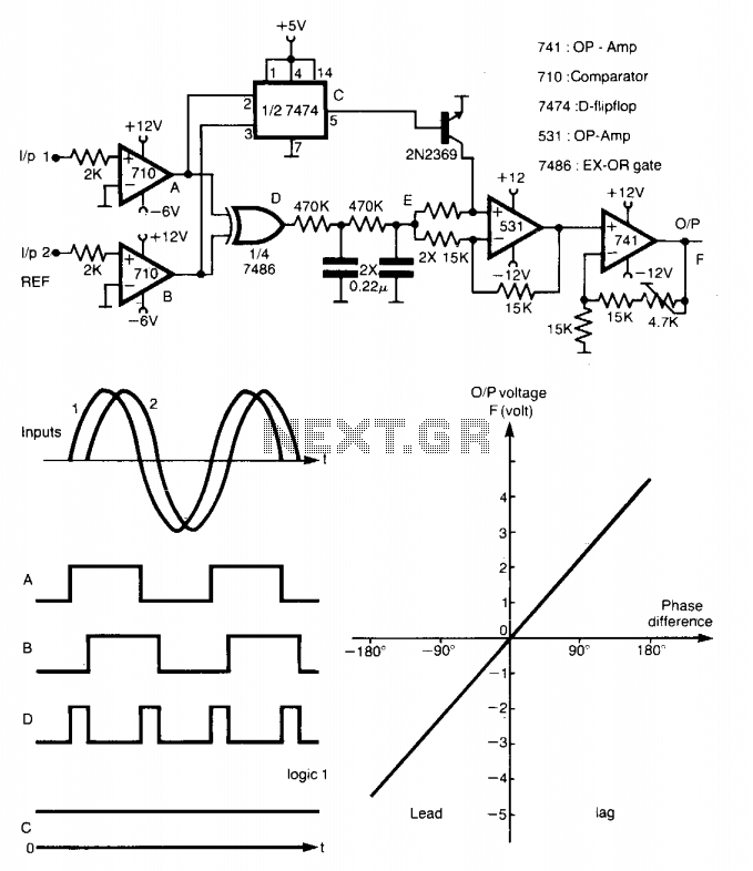
This method is capable of measuring the phase between 0 to ±180°. The generated square waves A and B are fed to a D flip-flop, which produces an output C equal to logic 1 when input A leads input...
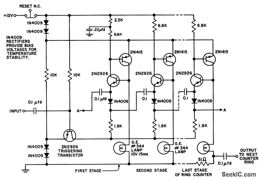
The circuit utilizes only six components per stage. By integrating counter and indicator functions, it achieves low battery consumption. Once the reset button is released, a 0.22 µF capacitor ensures that the first stage activates. Current is drawn by...
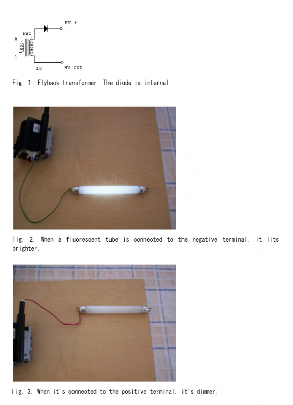
A high-voltage generator has been designed utilizing a flyback transformer as the output stage. The circuit diagram for the flyback transformer is illustrated in Figure 1. The high-voltage generator operates by converting low-voltage DC input into high-voltage AC output...
When the magnet approaches, the magnetic flux within the bifilar coil increases. An opposing magnetic flux is generated by the coil, resulting in an electromotive force (EMF) across inductors L1 and L2. The EMF across L1 applies a positive...