
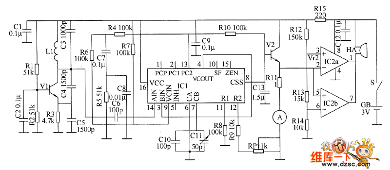
The FSK signal demodulation circuit composed of the digital phase-lock

The FSK demodulation circuit is designed to recover the original data signal from an FSK-modulated carrier wave. The digital phase-locked loop (PLL) serves as the core component of the demodulation process, providing synchronization between the input signal and the local oscillator. The two crystal oscillators, X and X2, generate stable reference frequencies that are essential for accurate demodulation.
In this configuration, the crystal oscillator X operates at a lower frequency of 983.04 kHz, while the higher frequency oscillator X2 at 1.2288 MHz allows for the effective shifting of the carrier frequency. The 74HC157, a quad 2-input multiplexer, is utilized for frequency conversion, enabling the selection of the appropriate frequency for demodulation based on the input signal characteristics. The frequency splitting circuit further divides the output frequency to facilitate the processing of the FSK signal.
Overall, the combination of these components within the circuit ensures precise demodulation of the FSK signal, allowing for reliable data recovery. The design emphasizes stability and accuracy, making it suitable for various communication applications where FSK modulation is employed.In Figure 7-2 is the FSK signal demodulation circuit composed of the digital phase-lock. The circuit consists of 2 oscillators with different frequencies, i.e crystal oscillators X (the frequency is 983.04KHz) and X2 (the frequency is 1.2288MHz) compose the oscillator, and X2 consists of the frequency converting circuit 74HC157, frequency splitting circuit.. 🔗 External reference
Related Circuits
A simple and effective antenna amplifier can be built using the provided circuit diagram. This amplifier is designed for the frequency range of 35 kHz to 150 MHz. It utilizes transistors, offering a low non-linearity of 3 dB and...
This document presents plans for a simple ground plane antenna that is effective in the FM band (88-108 MHz). It is constructed from a small plastic disk. The 6 x 6 loop antenna, designed by Graham Maynard, is highlighted...
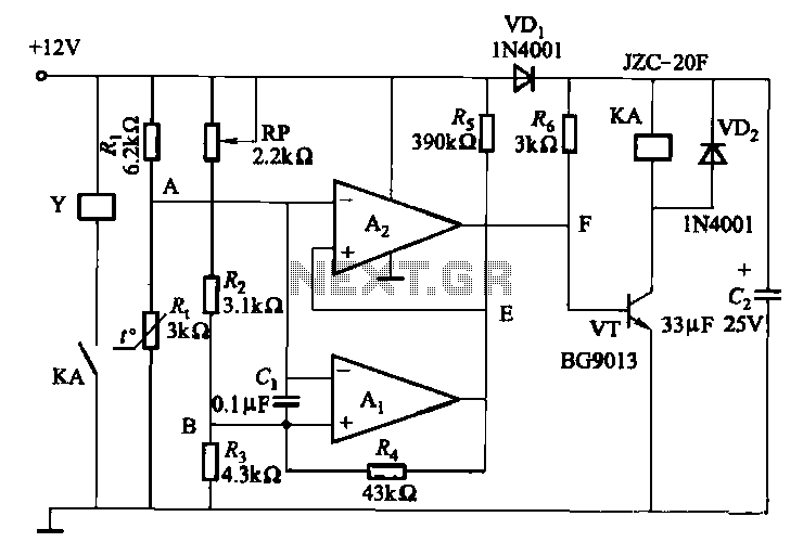
Electronic temperature control circuit for imported car air conditioners. It utilizes operational amplifiers A1 and A2, specifically the LM393 model. An adjustment potentiometer (RP) is included, allowing modification of the temperature range. The adjustment range includes a power temperature...
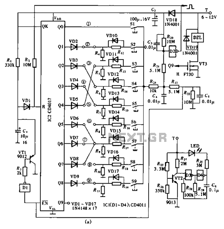
The lock circuit utilizes a decimal counter CD4017, which consists of ten output terminals. These terminals are connected through a combination that corresponds to a group of passwords, allowing for a maximum of up to 100 million combinations, hence...
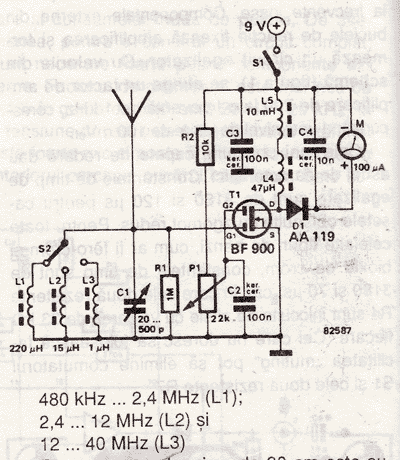
An RF field indicator is needed to verify power stages and transmitter antennas. This radio field indicator allows for the measurement of radiated energy from antennas. An RF field indicator is a crucial device in the field of telecommunications and...
The metal detector circuit consists of a probe oscillator, a PLL (phase-locked loop) circuit, and an audio alarm circuit. The probe oscillator includes a detection coil (L), transistor (V1), and several resistors (R1 to R3) and capacitors (C1 to...