
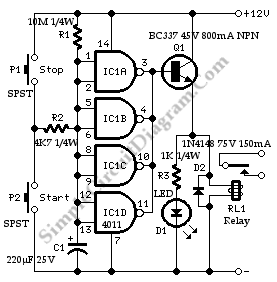
Time Switch

This circuit design incorporates various electronic components to create a reliable alarm system that can control the operation of multiple devices based on a preset time. The use of NAND gates for the S-R latch allows for stable toggling between the two modes, ensuring that the user can easily switch between activating and deactivating their devices. The incorporation of diodes protects the circuit from back EMF generated by the relay, while the transistors serve as efficient switches, minimizing power loss during operation. This design is particularly useful in scenarios where traditional alarm systems may fall short, providing a robust solution for waking users effectively.This circuit is especially designed for those who often need to wake up early in the morning. Ordinary alarms in electronic watches are not loud enough and very often they fail to wake up. The switch circuit described here will come handy; it can be used to switch on a TV, radio or tape recorder etc, which will not allow even the laziest amongst u s to ignore their sound for too long. Besides, this time switch can also be used to switch on/off any other electric or electronic gadget at any time. What you need is a simple analogue electronic clock with alarm facility and a small circuit to implement the time switch.
This time switch has two modes. One is time-on` mode and the other is time-off ` mode. In time-on mode, you set up the alarm in your clock as per normal procedure and at the set time this switch turns on the gadget connected at the output socket-1. In time-off mode, it turns your gadget off at the set time. The optional output socket-2 is wired in such a way that when you use this socket, the mode changes without having to flip the mode switch (i.
e. mode switch can be omitted). Please refer to the back panel diagram of a typical analogue clock and the audio jack, to see how the existing buzzer of the clock is required to be wired to the audio output from the clock. This will ensure that when plug is inserted in the audio jack, the clock`s buzzer will remain off and not consume any power unnecessarily.
The audio alarm output from the clock is coupled to the AF detector built around low-power switching transistor T1. During alarm, the collector of transistor T1 will fluctuate around ground level and Vcc. During absence of audio alarm input, the collector of transistor T1 is held at Vcc potential. The next stage consists of an S-R latch built around NAND gates N1 and N2. Capacitor C2 and resistor R4 are used for power-on-reset. On switching the power supply, gate N2 output will acquire logic 1 and that of gate N1 logic 0. This is the initial state, irrespective of the position of mode switch. At the time of alarm, when point A connected to collector of transistor T1 passes through logic 0 state, the output logic state of both the gates will toggle.
Assuming that mode switch is flipped to Mode Off` position at power-on-reset (when point D is at logic 1), initially diode D1 would be in blocking state and transistor T2 would be forward biased via resistor R5 and diodes D2 and D3. As a result, the relay is in energised state, which makes output power available at output socket1 and cuts it off from socket-2.
At alarm time, the audio signal toggles logic output states of both gates N1 and N2. As a result, point D goes to logic 0 state. Diode D1 conducts, taking the voltage at junction of diodes D1 and D2 to near about 1 volt. Diode D3 ensures that its series combination with diode D2 puts them in blocking mode. Capacitor C3 meanwhile discharges via resistor R6 and the voltage at base of transistor T2 approaches towards ground level, cutting off transistor T2 and de-energising relay RL1. Now the power at output socket-1 would be cut off while it becomes available in socket-2. If the above operation is repeated with switch S1 in Mode On, ` the power would initially not be available in socket-1 (but available in socket-2).
But after the alarm, the power would become available in socket-1 and not in socket-2. 🔗 External reference
Related Circuits

This circuit allows multiple cameras to be connected to a single monitor. It can be operated either manually or automatically. In automatic mode, a switch is connected to the output of a 555 astable multivibrator, which generates a continuous...

The duration for which the circuit remains active is determined by the time required for the stored electrical current to leak back into the circuit, which keeps the transistor and the entire circuit energized. A resistor is present that...
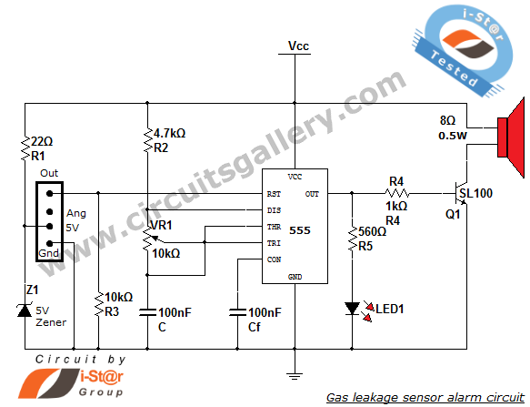
This article discusses a home security alarm circuit designed to detect LPG gas leakage. The circuit utilizes a gas sensor module, SEN 1327, which incorporates a QM 6 gas sensor. The output signal from this gas sensor module is...
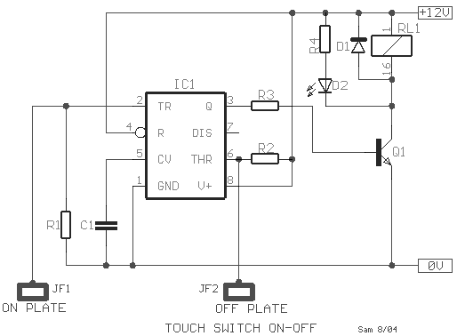
This type of sensor switch is ideal for creating touch-operated bells and buzzers in small toys, which function for a limited duration before automatically shutting off. The trigger's input impedance is very high, allowing the touch sensor switch to...

This low-voltage, high-current output switching power supply operates from a 220-V AC input. The circuit employs an ST2 diac relaxation oscillator, Q3, C1, and the diac to initiate conduction of the output switching transistor Q1. The on-time of Q1...
A very long time constant is provided by R1 and C1. C1 discharges, and the near-zero voltage at its positive lead is applied to the high-impedance inputs of the circuit. In this circuit, the combination of resistor R1 and capacitor...