
USB Cellphone Charger circuit

The circuit design described is a practical solution for charging mobile phones via a USB connection. The core components include a medium-power NPN transistor, a Zener diode for voltage regulation, and a protection diode to prevent reverse polarity connections. The NPN transistor acts as a voltage regulator, ensuring that the output remains stable at the desired level of 4.7 volts, which is essential for the proper functioning of lithium-ion batteries.
The circuit's input is connected to a Type A USB plug, which is a standard interface for USB devices. Careful attention to polarity is necessary, as incorrect connections can lead to battery damage. The Zener diode plays a critical role in maintaining output voltage; however, its removal could still allow the circuit to function under certain conditions, albeit without regulation.
The output connection should be made to a compatible charger pin that interfaces with the mobile phone's charging port. This design is particularly suited for hobbyists and individuals looking for a low-cost solution to charge their mobile devices from a USB power source.
The circuit can be tested using a multimeter to ensure that the output voltage is within the acceptable range before connecting it to a mobile device. This precaution helps to prevent any potential damage to the phone's battery. Overall, this USB cellphone charger circuit is a straightforward and effective method for charging mobile phones, particularly in scenarios where conventional chargers are unavailable.You can charge your Mobile Phone from the USB outlet of PC. This simple usb cellphone charger circuit can give regulated 4. 7 volts for charging the mobile phone. USB outlet can give 5 volts DC and 100 mA current which is sufficient for the slow charging of mobile phones. Most of the Mobile Phone battery is rated 3. 6 volts at 1000 to 1300 mAh. These battery packs have 3 NiMh or Lithium cells having 1. 2 volt rating. Usually the battery pack requires 4. 5 volts and 300-500 mA current for fast charging. But low current charging is better to increase the efficiency of the battery. The circuit described here provides 4. 7 regulated voltage and sufficient current for the slow charging of the mobile phone. Transistor T1 is used to give the regulated output. Any medium power NPN transistor like CL100, BD139, TIP122 can be used. Zener diode ZD controls the output voltage and D1 protects the polarity of the output supply. Front end of the circuit should be connected to a A type USB plug. Connect a red wire to pin1 and black wire to pin 4 of the plug for easy polarity identification. Connect the output to a suitable charger pin to connect it with the mobile phone. After assembling the circuit, insert the USB plug into the socket and measure the output from the circuit. If the output is OK and polarity is correct, connect it with the mobile phone. T1 & D1 will drop approx 0. 7 volts each, so 5V (usb) min 1. 4 volts will drop too much volts. More over it is mentioned if input polarity is wrong then battery will be damaged. In presence of D1 reverse volts will be blocked then how it can damage battery. Clarification of these facts required please Most Mobile battery is rated between 3. 2 to 3. 6 volts. Even if T1 and D1 drops voltage, sufficient voltage will be available to charge the battery. If required, ZD can be eliminated. But there will not be any regulation. D1 act as the polarity protector. But if the mobile battery terminal is connected in reverse, positive terminal of the battery goes to the negative of USB.
This may harm the battery I like your learned comments on the site. I am an electronics hobbyist (just begun). I want to make a dual power source cellphone charger. Source 1. 240 V AC supply I like your learned comments on the site. I am an electronics hobbyist (just begun). I want to make a dual power source cellphone charger. Source 1. 240 V AC supply 1. Your answer to Iftikar Ahmad is not convincing at all. The base emitter junction of T1 together with the diode D1 will drop 1. 2V, so the final voltage at the output will be 3. 2V, which is definitely not enough to charge a Li-On cellphone battery. And the output voltage shown in the schematic is 4. 7V, such a blatant mistake! 2. You mention that removing the zener diode will result in no regulation! I hope you are aware that the USB socket of any PC gives out REGULATED 5V DC. SO removal of the zener will not affect the regulation at all. 3. Lastly, the whole circuit just does not serve any purpose at all, since the easiest way to charge a mobile phone battery is to directly connect it to the USB socket of a PC, the regulated 5V DC will charge the battery. Cool, isn`t it 1. If it were the base emitter then your current flow would also need to go through R1 which would really drop the voltage.
Unless I am mistaken (it has been 5 year since I was into this type of stuff) the collector/emitter is the real voltage drop that we are concerned with as far as the voltage drop is concerned. This voltage drop is actually around 0. 2V. So that raises it to a respectable 4. 1V output if you have a 5V supply. Still not the 4. 7 he was going for but it might work for some phones. 3. I recently (the reason I`m even looking this stuff up)had my charge port on my phone go out and wanted a quick, and cheap alternative to buying a new phone or wall charging dock.
This wont work for me but it was a fun mental exercise. Well V 🔗 External reference
Related Circuits
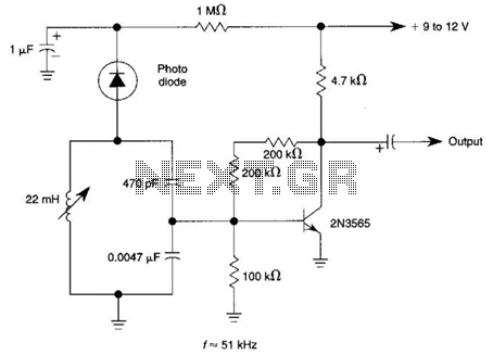
The circuit utilizes a tuned circuit for frequency selection, designed to operate at approximately 51 kHz. The 2N3565 transistor amplifies the output generated by the tuned circuit. The described circuit operates on the principle of resonance, where the tuned circuit...
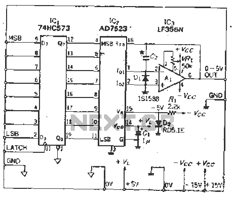
The IC latch is utilized to hold the digital data when the clock signal rises. The configuration includes a holding data port AD7s23, a thin film resistor ladder, and a switch that together form an 8-bit Digital-to-Analog Converter (DAC)....

A combined monostable multivibrator using the 555 timer integrated circuit, along with a pair of light control comparators. This circuit can be utilized to control a load based on the timing parameters set within the circuit. The circuit comprises a...
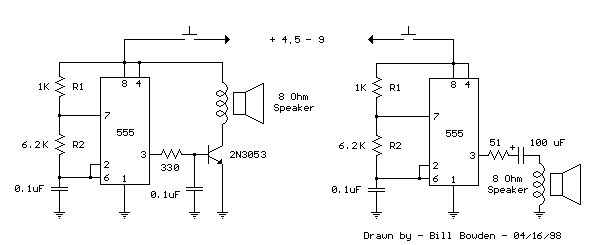
This is a basic 555 square wave oscillator used to produce a 1 kHz tone from an 8-ohm speaker. In the circuit on the left, the speaker is isolated from the oscillator by an NPN medium power transistor, which...
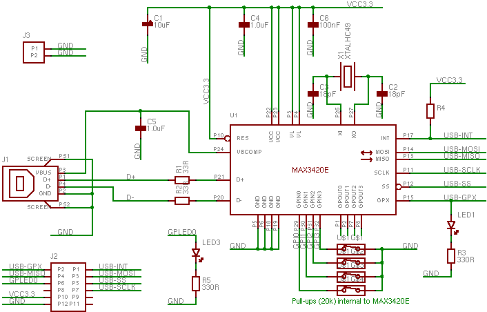
The MAX3420 is a USB peripheral controller chip featuring an SPI bus. This document aims to provide sufficient information for effective utilization of the device in various projects. The MAX3420 simplifies the integration of a USB interface into a...

This sensor switch circuit features nine channels and consists of three integrated circuits along with several resistors. The 74HC147, which has a high input impedance, enables the use of 4.7 MΩ resistors to establish a logic level "high" for...