
Very high current power supply

This switching inverter design is particularly useful in applications requiring high current output while maintaining low voltage levels. The push-pull topology is advantageous for its efficiency and simplicity in implementation. The transformer plays a crucial role in maintaining the desired voltage transformation while allowing for significant current amplification. The selected MOSFETs must be capable of handling the high voltage and current demands, with careful attention to their on-resistance to minimize heat generation during operation. The use of Schottky diodes for rectification is beneficial due to their low forward voltage drop, which contributes to overall efficiency.
In terms of thermal management, adequate heat sinks and cooling mechanisms must be incorporated to ensure reliable operation, particularly during continuous use. The design's ability to operate at a frequency of 40kHz allows for compact transformer designs and reduced component sizes, which is advantageous for applications with space constraints. The flexibility to modify input parameters and adapt the design for different operational scenarios enhances its utility across a range of high current applications. Overall, this schematic represents a robust solution for generating high current low voltage power supplies in various industrial and experimental settings.Sometimes you need a low voltage power supply of very high currents (hundreds of amperes) - whether for spot welding, heating or melting metals, starting the vehicle engine, or other physical experiments. Such a supply I have now decided to build. Given that I already have a switching power supply 3-60V 40A and 60A 56V power supply, so I desided t
o build a switching inverter that which will change the DC voltage of up to 60V to a smaller voltage to approximately 12V at a higher current. I chose the topology of push-pull that uses a transformer with 5:1 ratio. Voltage regulation (if necessary) and current limit are provided by a source of input voltage. This switching inverter reduces the input voltage of approximately 5:1 ratio minus the lossed and voltage drops (diodes, MOSFETs, winding and conductors resistance), in practice it is up to 6:1.
In almost the same rate, thw inverted increases the allowable current. For 40A input source you can get about 200 - 240A. The highest output voltage of this high current switching inverter is about 10-12V. The schematic diagram of the described switching inverter is shown below. Transformer Tr1 has primaries 5+5 turns and secondaries 1+1 turn. Switching is provided by 4 + 4 MOSFETs. I used IXFH50N20 type (50A, 200V, 45mR, Cg = 4400pF). You can use any voltage MOSFETs with Uds 200V (150V) and the least conductive resistance. The speed and smaller capacity (charge) of gate are also not bad. Secondary rectification is provided by two double Schottky diodes MBRP60035CTL (600A, 35V). Ferrite transformer Tr1 has the cross section about 15 x 15 mm. Inductor L1 is formed by 5 iron powder rings threaded on wires. Inductance, radiator and some other parts I got from some old inverter 56V / 5V (hundreds of A), that was used for information technology. I used the original snubbers on the power board. I disconnected the gates from the original circuit (unusable) and hooked to my own control circuit. It uses an integrated circuit IR2153. Due to the large capacity of gates (4x 4n4), I had to use a power amplifier with a pair of NPN / PNP transistors BD139 and BD140.
However, the IR2153 circuit can be replaced by other control circuit allows pulse width modulation (PWM), for example, SG3525, to create a regulated source. It is theoretically possible to change the input voltage (other MOSFETs, primaries, etc. ) and even work directly with a rectified mains. This switching supply topology provides galvanic isolation. Warning - MOSFETs sees twice the input voltage (at 60V it is 120V and in case of rectified 230V~ mains it would be 650V).
Operating frequency is about 40kHz. In the short term use (eg as a vehicle engine starting source, spot welder) are not so great demands on the cooling, winding sizing, etc. In continuous operation, good cooling is necessary. Greatest power loss occurs at the output diodes. Schottky voltage drop is about 0. 5 V and a current for example 240A gives its loss of 120W. 🔗 External reference
Related Circuits
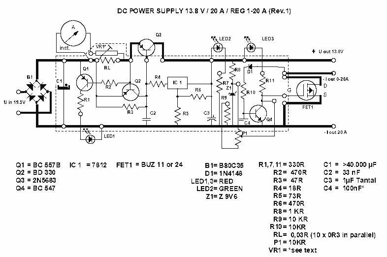
This PSU has been especially designed for current-hungry ham radio transceivers. It delivers safely around 20Amps at 13.8V. For lower currents, a separate current limiting output, capable of 15ma up to a total of 20A has been added. Let...
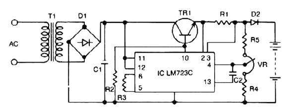
This power supply circuit operates using 120 volts from household mains and should only be undertaken by individuals with the appropriate knowledge and skills to safely construct such a project. Failure to do so may result in personal injury...
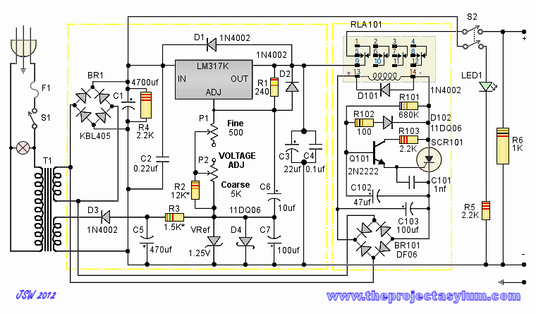
Constant Voltage Current Limited Charger power supply. Refer to the page for an explanation regarding the associated circuit diagram. The Constant Voltage Current Limited Charger power supply is designed to provide a stable output voltage while limiting the current to...
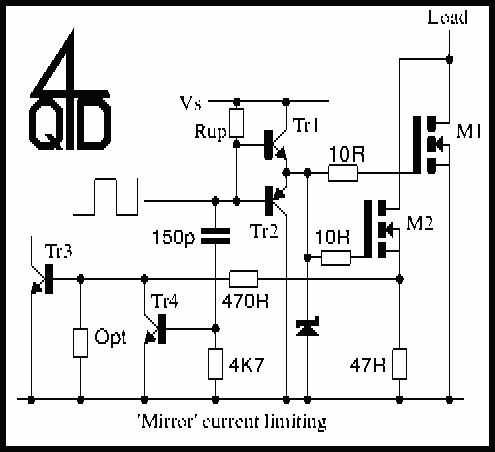
The circuit shows the method of mirror current sensing a MOSFET. A fully conducting MOSFET is resistive and behaves exactly as a resistor. It therefore you limit the voltage across the MOSFET when it is conducting you automatically limit...
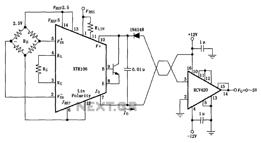
The IN4148 series diode is connected in the V+ line and configured in a loop to prevent damage from reverse voltage conditions. The diode exhibits a forward voltage drop of approximately 0.7V, which affects the supply voltage. The circuit...
This circuit is a class AB stereo audio power amplifier designed by Quasar for high-fidelity applications using a TDA2005 module. It is straightforward to construct and requires a minimal number of external components. The module includes output current protection...