
VFC110: Single Chip High-Frequency Voltage-to-Frequency Converter (VFC)
")
The VFC110 voltage-to-frequency converter is designed to convert an analog voltage input into a frequency output, making it suitable for various applications requiring frequency modulation of voltage signals. The high-frequency capability of the VFC110 enables it to handle input voltages ranging from 0V to 10V, translating this range into a frequency output from 0 Hz to 4 MHz.
The chip's internal architecture includes a precision 5V reference, which is crucial for maintaining accuracy in the conversion process. This reference voltage can be used to calibrate the output frequency, ensuring that the converter operates within specified tolerances. The disable function allows for power management by turning off the chip when not in use, thus reducing power consumption.
The output stage, designed as an open collector, allows for easy interfacing with other digital circuits. This configuration means that the output can be connected to various logic families, including TTL and CMOS, making the VFC110 versatile for integration into different electronic systems.
For the circuit design, the use of a pull-up resistor is essential for ensuring that the output signal is pulled to a high state when the open collector output is not actively driven low. The inclusion of two bypass capacitors is vital for filtering power supply noise, which can adversely affect the performance of the voltage-to-frequency conversion. The recommended 100nF mylar capacitors are effective in providing stable power supply conditions, enhancing the reliability of the converter's output.
Overall, the VFC110 chip represents an efficient solution for converting voltage levels into corresponding frequency signals, suitable for applications in signal processing, sensor interfacing, and data acquisition systems.Using VFC110 chip, we can build a high frequency voltage-to-frequency converter. The features of this chip include the capability of high frequency operation, disable function, and an on-board precision 5V reference. This precision reference can be used to provide reference for offsetting the VFC transfer function, as well as provide transducer or
bridge excitation. As well as shutting off the single VFC chip, Multiplexing several VFC outputs can be done by the enable function. The output is an open collector stage that is compatible with TTL or CMOS logics. Here is the schematic diagram of the circuit: You can see that this circuit only use a pull up resistor for the output and two bypass capacitors for power supply filtering.
You can use a 100nF mylar cap for these two bypassing capacitors. Using minimum the component count, this circuit provide 0-4MHz output for 0-10V input voltage. [Circuit`s schematic diagram source: Texas Instruments Application Notes] 🔗 External reference
Related Circuits
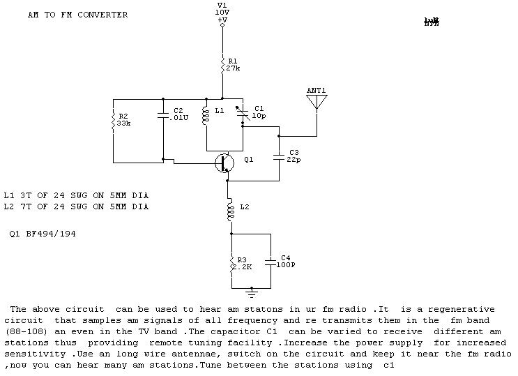
The circuit described is designed to enable the reception of AM stations on an FM radio. It operates as a regenerative circuit, sampling AM signals across various frequencies and retransmitting them within the FM band (88-108 MHz) and even...
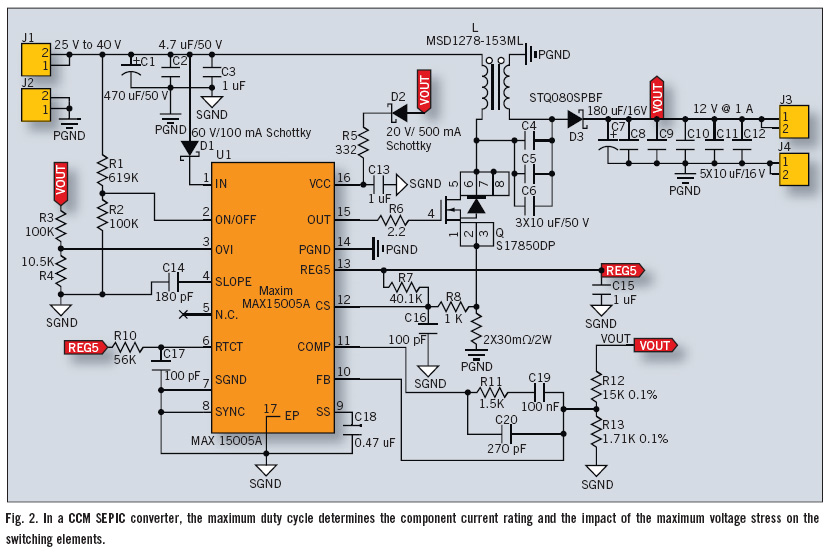
The Single-Ended Primary Inductance Converter (SEPIC) topology is an effective solution for automotive power systems that necessitate an output voltage that falls between the low and high values of the input voltage. The SEPIC topology is suitable for this...
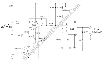
A voltage-to-frequency converter (VFC) circuit is illustrated in the schematic diagram below. The circuit utilizes a 555 integrated circuit (IC) as the central component of its operation. The voltage-to-frequency converter (VFC) is a crucial electronic circuit that converts an input...
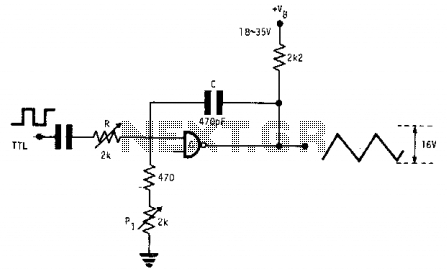
This fixed-frequency triangular waveform generator, driven by a TTL square wave, produces triangular waveforms with a peak-to-peak voltage of typically 16 V at frequencies reaching several MHz. The design utilizes a single AND open collector gate or an open...

The ICL7134B circuit is a bipolar input analog-to-digital (A/D) converter that employs two AM25L03 chips to create a 14-bit successive approximation register. The comparator features a two-stage amplifier, HA2605, which is utilized to mitigate settling time issues at the...

The CN3052A/CN3052B/CN3056 is a high-performance linear lithium battery management chip. It integrates a power transistor, eliminating the need for an external sense resistor and a choke flow diode for current sensing. Only a few peripheral components are required, and...