
Video Fader Circuit

The proposed circuit utilizes two LT1228 transconductance amplifiers, which are configured to operate in a manner that allows for precise control over the video signal levels. The LT1228 is known for its high-speed performance and low distortion, making it suitable for video applications. In this configuration, both amplifiers are connected in such a way that they modulate the current flowing into a subsequent current feedback amplifier.
The operation of the video fader relies on the principle of current summation at the output. Each LT1228 amplifier receives an input signal, and the gain of each amplifier can be adjusted by varying the currents fed into pin 5. This pin is critical as it sets the transconductance of the amplifier, thereby controlling the output current proportional to the input voltage. By manipulating these set currents, the user can achieve a desired ratio of the input signals, effectively fading one video signal into another.
The current feedback amplifier then combines these outputs, providing a final video signal that reflects the desired blend of the two input signals. The design allows for smooth transitions between video sources, making it ideal for applications in video production and broadcasting where seamless switching is required. The circuit can be further enhanced with additional components, such as filters or buffers, to optimize performance based on specific application needs.
Overall, this configuration of LT1228 amplifiers and a current feedback amplifier presents a robust solution for implementing a video fader, ensuring high fidelity and responsiveness in video signal processing. Using two LT1228 transconductance amplifiers in front of a current feedback amplifier forms a video fader. The ratio of the set currents into pin 5 determines the ratio of the inputs at the output.
Related Circuits
A substation capable of consuming 100 MVA with 375 kVA, 60 Hz input and 132 kV at 50 Hz using the same power. The challenge is to convert the 60 Hz input to 50 Hz, including a wiring diagram. To...
At low output power, up to 18 W, the device functions as a standard BTL amplifier. When a greater output voltage swing is necessary, the internal supply voltage is increased using external electrolytic capacitors. This momentarily elevated supply voltage...

This is a BTL (bridged tied load) mono amplifier with a DC volume control circuit. This circuit utilizes the TDA7052A/AT, which is suitable for monitors, TVs, and battery-operated portable radios and recorders. Unlike conventional DC volume circuits, the TDA7052A/AT...
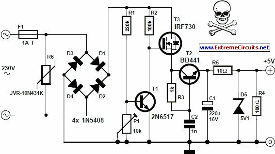
An increasing number of appliances draw a very small current from the power supply. If designing a mains-powered device, one can generally choose between a linear and a switch-mode power supply. However, when the appliance's total power consumption is...
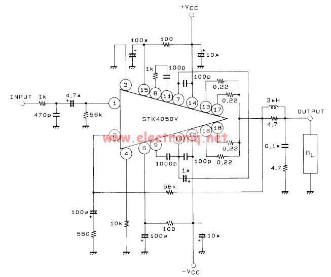
This 200-watt audio amplifier circuit diagram is based on the STK4050V high-power audio amplifier IC, designed to deliver up to 200 watts of audio power on a single channel. The STK4050V 200-watt audio amplifier circuit is pin-compatible with other...
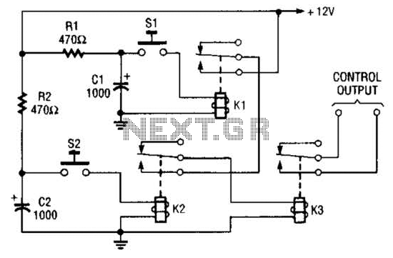
Due to the limited hold-on time of the delay circuits R1/C1 and R2/C2, both switches S1 and S2 must be activated simultaneously to energize the load. The circuit in question involves a delay mechanism governed by the time constants associated...