
Video Fader Circuit

To effectively fade a video signal while maintaining the integrity of the synchronization components, a more sophisticated approach is required. This can be achieved through the implementation of a dedicated fading circuit that selectively attenuates the luminance (Y) and chrominance (C) components of the video signal, while preserving the timing information.
A common method involves the use of a voltage-controlled amplifier (VCA) for the luminance signal and a separate VCA for the chrominance signal. These components can be controlled by a common control voltage that dictates the fade level. The synchronization pulses, which are embedded within the composite signal, must be extracted and treated separately to ensure they remain at an acceptable amplitude throughout the fading process.
The circuit can be designed using operational amplifiers configured as inverting or non-inverting amplifiers, where the gain can be adjusted based on the control voltage. A low-pass filter may also be integrated to smooth out any abrupt changes in the signal, which can lead to visual artifacts.
In addition, a feedback mechanism can be implemented to monitor the output levels of the synchronization signals, ensuring they do not drop below the required thresholds. This can be achieved using comparators that trigger an alarm or adjust the control voltage dynamically if the sync pulses approach critical levels.
In summary, fading a video signal requires careful handling of both the luminance and chrominance components, as well as the synchronization signals, to ensure a seamless transition without degradation of the signal quality. Proper circuit design, including the use of VCAs and feedback mechanisms, is essential to achieve the desired result.Fading a video signal can`t be done simply by attenuating the composite signal, since the synchronization signal may drop below unacceptable level. Here a . 🔗 External reference
Related Circuits
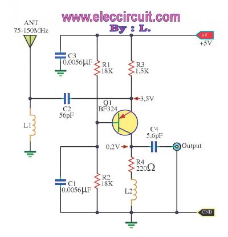
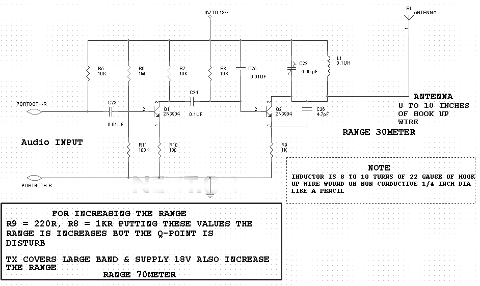
This is a wideband high-frequency amplifier circuit designed for a frequency range between 75-150 MHz. It utilizes a PNP transistor amplifier to enhance signal strength before it reaches the receiver of devices such as phones, FM radios, or amateur...
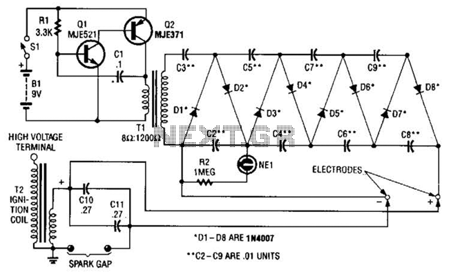
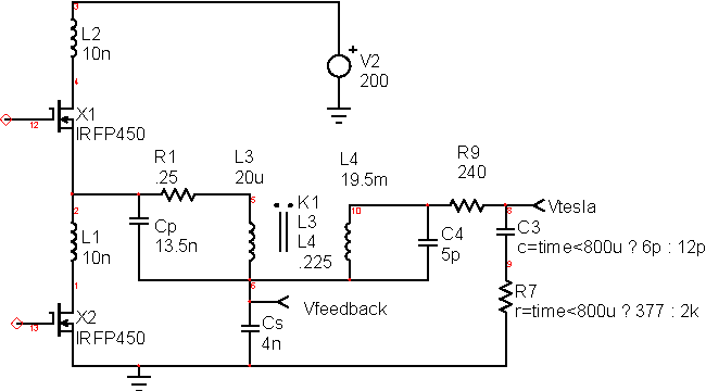
This circuit employs a transistor oscillator and a voltage multiplier to charge capacitors CIO and CI1 to a high voltage. When the spark gap breaks down, T2 generates a high-voltage pulse through the discharge of capacitors CIO and CI1...
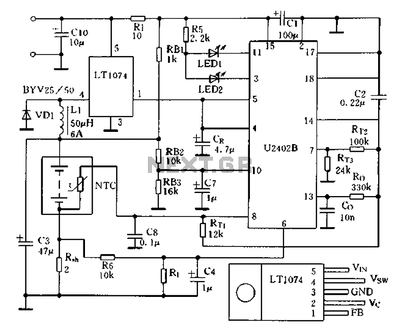
Charging circuit from the DC power supply switching power supply control The charging circuit described is designed to operate with a DC power supply, utilizing a switching power supply control mechanism. This type of circuit is commonly employed in applications...
877 ~ 924MHz RF2152 power amplifier circuit diagram. The RF2152 is a high-performance power amplifier designed for applications in the 877 to 924 MHz frequency range. This amplifier is typically used in various RF communication systems, including wireless networks and...
This schematic is directly sourced from the Altera ByteBlaster datasheet or manual, which provides comprehensive details regarding the connector's functionality and pin connections. It is advisable to review the datasheet available on their website or through a search engine...
Due to the low coupling coefficient, the primary self-inductance tends to short out the driving signal. However, utilizing a series/parallel set of capacitors for energy coupling increases the input impedance at resonance, thereby achieving good power transfer efficiency. The...