
Voltage Controlled Oscillator using NE555

The NE555 timer is a versatile integrated circuit widely used in various applications, including oscillators, timers, and pulse generation. In the context of a voltage-controlled oscillator (VCO), the NE555 can be configured in astable mode, allowing it to generate a continuous square wave output whose frequency is dependent on the voltage applied at pin 5.
The circuit typically consists of the NE555 timer, a timing capacitor (C1), two resistors (R1 and R2), and a potentiometer (P1) to adjust the control voltage. The resistors R1 and R2 form a voltage divider that sets the threshold levels for the NE555. The timing capacitor C1 determines the charge and discharge time, which directly influences the output frequency.
When a voltage is applied to pin 5, the internal voltage divider of the NE555 adjusts the timing intervals based on the control voltage. The relationship between the control voltage and the output frequency is inversely proportional; as the control voltage increases, the frequency decreases due to the longer charge and discharge times of the capacitor.
It is essential to select appropriate values for R1, R2, and C1 to achieve the desired frequency range. The output frequency (f) can be calculated using the formula:
\[ f = \frac{1.44}{(R1 + 2R2) \times C1} \]
In this configuration, the potentiometer allows fine-tuning of the control voltage, facilitating precise frequency modulation. The output from the NE555 can be utilized to drive loads directly or can be fed into subsequent stages of a circuit, such as filters or amplifiers, depending on the application requirements.
This voltage-controlled oscillator circuit is particularly useful in applications requiring frequency modulation, such as in communication systems, signal generators, and audio synthesis, where varying the frequency in response to an input control voltage is necessary.A voltage-controlled oscillator using NE555 The circuit is usually known as a voltage-to-frequency converter as a result of the output frequency will be modified by changing the input voltage. As mentioned in previous blog posts, pin 5 terminal is voltage control terminal and its function is to manage the edge and trigger levels.
Normally, the con trol voltage is +2/3VCC because of the inner voltage divider. However, an external voltage will be applied to the current terminal directly or through a pot, as illustrated in figure, and by adjusting the pot, control voltage can be varied. Voltage across the timing capacitor is depicted in figure, that varies between +Vcontrol and ½ Vcontrol.
If control voltage is increased, the capacitor takes a extended to charge and discharge; the frequency, therefore, decreases. so the fre quency will be modified by changing the control volt age. Incidentally, the control voltage is also created offered through a pot, or it should be output of a transistor circuit, op-amp, or another device.
🔗 External reference
Related Circuits
This is an astable multivibrator (oscillator) circuit utilizing a CMOS inverter. The circuit employs the CD4007 or MC14007 components. It operates within a frequency range of... The astable multivibrator circuit is designed to generate a continuous square wave output without...
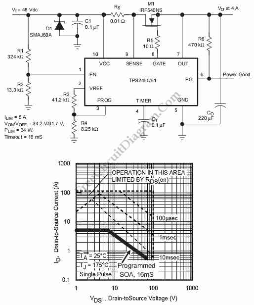
This is a positive high-voltage hot swap controller circuit with a power limiter. This circuit utilizes the TPS2491 or TPS2490, as both of them have specific features. The positive high-voltage hot swap controller circuit is designed to safely connect and...
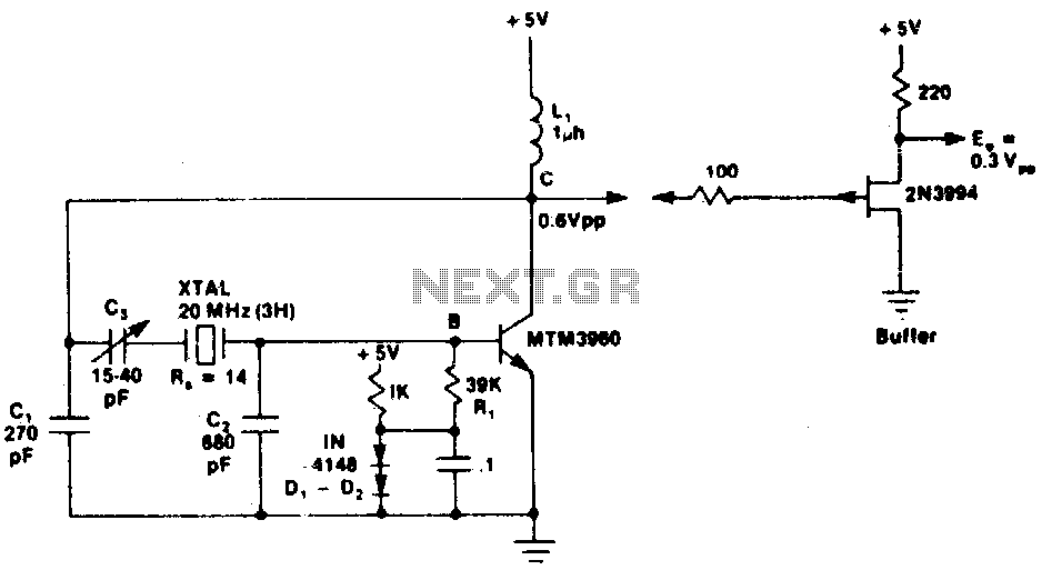
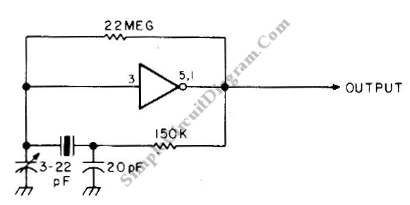
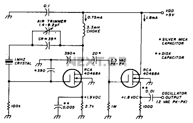
This circuit exhibits excellent short-term frequency stability due to the external load connected across the crystal, which is predominantly capacitive rather than resistive. This configuration results in a high in-circuit quality factor (Q) for the crystal. The circuit utilizes a...
Neural networks are a broad topic. This example demonstrates how to create a basic neural sensor that takes resistive readings from multiple sensors, multiplies them by a weight factor, and then sums the results. The results are compared to...
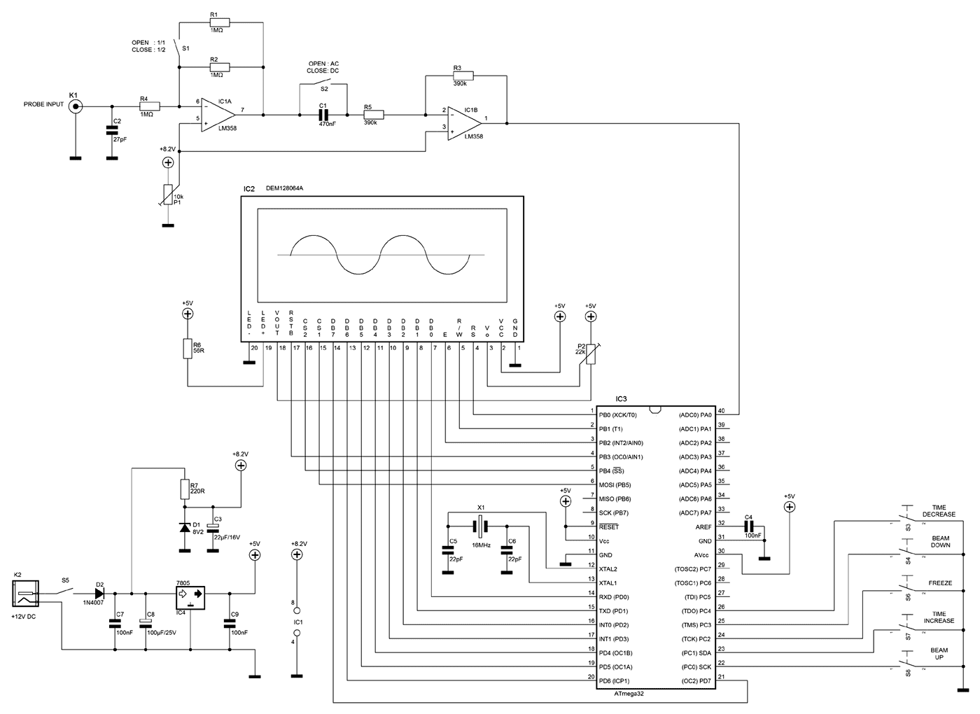
A few months ago as I was surfing on the net, I saw an oscilloscope based on PIC18F2550 microcontroller and a KS0108 controller based graphical LCD. That was Steven Cholewiak's web site. I had never seen before so amazing...
This stable oscillator circuit exhibits less than a 1 Hz frequency change over a VDD range of 3 to 9 volts. Stability is attributed to the use of MOSFET devices and stable capacitors. The described oscillator circuit is designed to...