
Wien bridge sine wave oscillator

The circuit employs the 2N5457 JFET, a junction field-effect transistor known for its high input impedance and low noise characteristics. In this configuration, the JFET is integrated into the feedback loop of an amplifier, where it acts as a variable resistor. By adjusting the gate voltage of the JFET, the resistance can be modulated, allowing for precise control over the feedback level. This modulation is crucial for maintaining a low distortion output while ensuring that the amplitude of the sine wave remains constant, which is essential for high-fidelity applications.
The LM103 zener diode is implemented to provide a stable voltage reference, which is critical for setting the peak amplitude of the sine wave. The LM103 is known for its low temperature coefficient and excellent voltage regulation, making it suitable for applications where precision is paramount. By using the LM103, the circuit can achieve a reliable reference voltage that helps maintain the desired output characteristics of the amplifier, ensuring that the sine wave peaks are consistent and free from fluctuations.
Overall, this circuit design effectively combines the properties of the 2N5457 JFET and the LM103 zener diode to create a robust amplifier configuration capable of delivering high-quality sine wave signals with minimal distortion. The feedback loop's design, along with the voltage reference provided by the zener diode, contributes to the overall performance and reliability of the amplifier system.Using the 2N5457 JFET as a voltage variable resistor in the amplifier feedback loop, produces a low distortion, constant amplitude sine wave getting the amplifier loop gain just right The LM103 zener diode provides the voltage reference for the peak sine wave amplitude.
Related Circuits

This circuit functions as an astable multivibrator, also known as an oscillator. The two transistors are interconnected in a manner that allows the circuit to alternate between two states. In one state, the base of transistor Q1 is approximately...

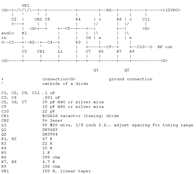
Oscillator, operates with 2 to 12 volts DC (optimal performance is achieved at 9 to 12 volts for maximum volume and clear keying). Additionally, R1 can be substituted with a 500K potentiometer, allowing the circuit to sweep across the...
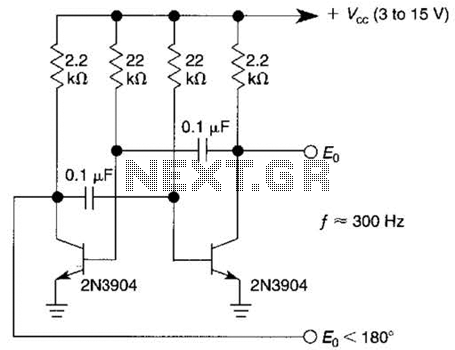
This free-running square-wave oscillator utilizes two NPN transistors. The output frequency is approximately 300 Hz with the specified component values. The circuit operates as a basic oscillator, generating a square wave output through the interaction of two NPN transistors. The...
The world is full of xtal oscillators twiddled by digital designers lacking in the analog design knowledge necessary. Just look at all the PC real time clocks that lags or leads by several minutes per day. And they eat...
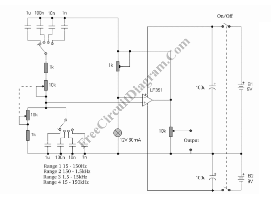
This sine wave generator is adjustable between 15 Hz and 150 kHz. The circuit is essentially a Wien-bridge oscillator, featuring multiple capacitor selections. The sine wave generator operates on the principle of the Wien-bridge oscillator, which is known for producing...
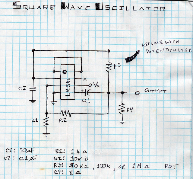
This is a square wave oscillator (digital, similar to 8-bit music). It is based on the LM386 amplifier integrated circuit, which is also the foundation for the mini guitar amplifier. The design includes a simple power switch connected to...