
Wireless doorbell 300MHz


The described circuit operates primarily at a frequency of 303MHz, utilizing a 2N3563 transistor, which is well-suited for RF applications due to its capability of handling frequencies up to 1,000MHz. This transistor is essential in ensuring that the oscillator maintains a good gain at the desired frequency of operation. The circuit is designed around a CD4069 integrated circuit, which contains six inverters that are configured to generate a 32kHz tone. The configuration of four gates in parallel is critical, as a single gate lacks the output drive necessary to pull the emitter of the transistor close to ground potential; however, four gates can effectively bring the emitter voltage near 0V, which is vital for maintaining oscillation.
The operational characteristics of the CD4069 are such that it toggles its output based on the input voltage relative to the mid-rail voltage. This behavior allows it to detect small analogue signals, making the circuit suitable for experimentation with RF and high-impedance components. The feedback mechanism, achieved by connecting a 1MΩ resistor from the output to the input of the gate, maintains the gate in an oscillatory state at approximately 500kHz. This oscillation is crucial for processing even the smallest input signals.
In the specific gate configuration between pins 13 and 12, the inclusion of a 1nF capacitor serves to significantly reduce the frequency, while additional components, such as a 2.2nF capacitor and a 5.6kΩ resistor, further shape the signal characteristics. The subsequent gates amplify the signal amplitude without filtering out unwanted noise. As a result, the signal at the crystal's left side is full amplitude but contains various noise components. The crystal acts as a selective filter, only allowing the 32kHz component to pass through, which is essential for triggering the oscillator and preventing false activations. The clean signal extracted by the crystal is then amplified to the supply voltage level, enabling it to charge an electrolytic capacitor that activates a sound chip.
To initiate oscillation, a resistor is strategically placed between the output and input, facilitating oscillation at the highest frequency range of the gate, which can vary between 500kHz and 2MHz. When an additional gate is introduced and connected to a crystal, the circuit experiences a competition between the oscillation generated by the resistor and the frequency dictated by the crystal. Since the crystal presents a lower impedance, it dominates the input signal at pin 11, allowing the gates to operate at the crystal's frequency, thereby stabilizing the oscillation and enhancing the circuit's performance.The operation of a 303MHz circuit has been covered in our project WIRELESS DOORBELL. We are not going over how the circuit works but explain the importance of some of the components and how they effect the range. The most critical component is the transistor. A quality transistor is important in the RF section and Japanese transistors are by far the best for this purpose.
The transistor used in the 303MHz oscillator has a maximum frequency of operation of 1,000MHz and this is where its gain is equal to "1," so we want a transistor to have a good gain at 300MHz. A BC 547 transistor will not operate at this frequency so we have used a 2N 3563 which is low cost and will operate up to 1,000MHz.
The following circuit uses a CD 4069 IC to produce the 32kHz tone and 4 gates in parallel to turn the oscillator transistor on and off at the tone-rate. A single gate will not have enough output to pull the emitter to ground, however 4 gates will bring the emitter close to 0v rail.
It must not be at exactly 0v as the 6p will not have an effect in maintaining oscillation. The chip has 6 gates and when an input is just above mid rail, the output goes LOW. When the input is just below mid rail the output goes HIGH. The gap between detecting a low and a high is not very large and the gate will detect signals called "analogue signals." This type of circuit makes an ideal basis for experimentation. You can experiment with the RF side of the circuit as well as the high impedance sections. Each gate is capable of providing a very high gain and by putting a 1M from output to input the gate is kept in a state of excitement, oscillating at approx 500kHz, if no other components surround the gate to control the frequency.
This is designed to keep the gate active so that the smallest signal will be processed. In the case of the gate between pins 13 and 12, the 1n capacitor between the input and ground will reduce the frequency enormously, as well as the effect of the 2n2 and 5k6 resistor. The second and third gates simply increase the amplitude of the signal and do not provide any form of removal of unwanted signals.
The end result is a full amplitude signal at the left-side of the crystal with all sorts of hash and background noise, but unless the signal has a 32kHz component, it will not start to oscillate and the right side will have no signal. The crystal is the component that does most of the "detection work" and prevents false triggering as it magically picks out the 32kHz signal from the "hash" and delivers a very clean signal to the transistor for further amplification.
This signal is amplified further to full rail and charges an electrolytic to activate a sound chip. But to get the oscillator circuit to start-up, a resistor is placed between output and input. This will produce an oscillation at the highest frequency for the gate about 500kHz to 2MHz.. When another gate is added and a crystal connected between the output and the input, a "fight" takes place between the signal produced by the 1M and the frequency delivered by the crystal. Since the crystal has a lower impedance than the 1M, it delivers a larger signal to input pin 11 and the two gates operate at the frequency of the crystal.
🔗 External reference
Related Circuits
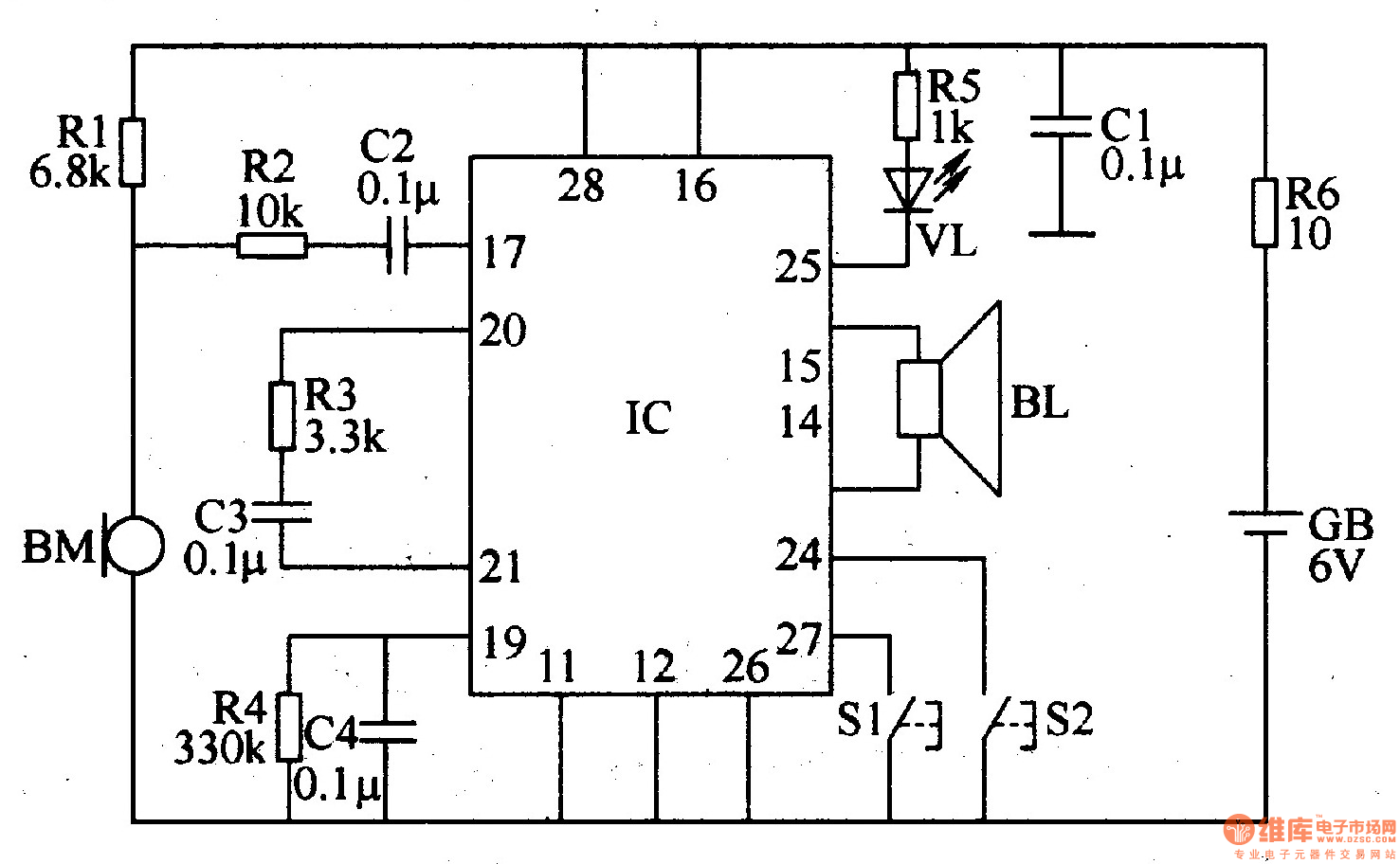
The recordable electronic doorbell consists of a recording and playback integrated circuit (IC), resistors R1-R6, capacitors C1-C4, a microphone (BM), a speaker (BL), control buttons S1 and S2, a battery (GB), and an LED (VL). Resistors R1-R5 should be...
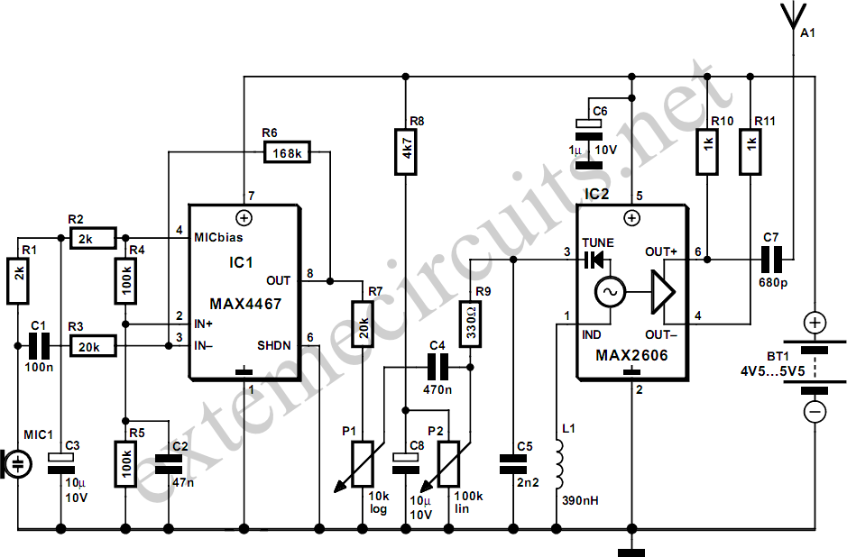
This project involves a simple and cost-effective transmitter designed for hobbyists and home experimenters, capable of transmitting speech over a short distance. It functions as a cordless microphone, utilizing two integrated circuits from Maxim. The first IC, MAX4467, acts...
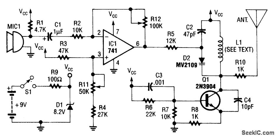
An operational amplifier integrated circuit (741) amplifies the audio signal from microphone 1 (MIC1), with resistor R12 determining its gain. The amplified audio signal is then directed to the oscillator circuit, which includes transistor Q1 and associated components. D2...
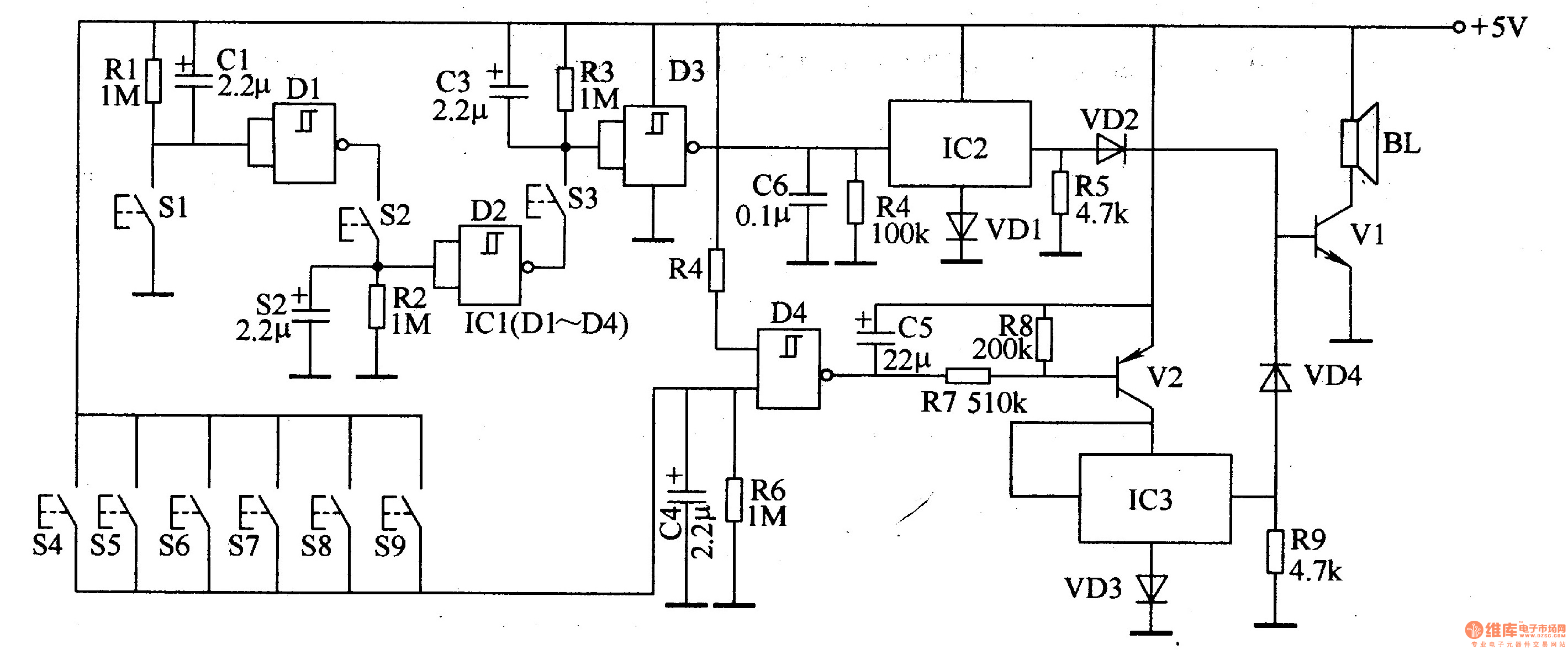
The password electronic doorbell circuit comprises a trigger circuit and a music generating circuit, as illustrated in Figure 3-119. The trigger circuit includes buttons S1-S9, four NAND gate Schmitt trigger integrated circuits (IC1), and external RC components. The music...

Sustainable satellite 802.11b wireless internetwork and how it was achieved. The design of a sustainable satellite 802.11b wireless internetwork involves the integration of satellite communication technology with wireless networking standards to create a robust and efficient communication system. This architecture...
The intersection of industry and data collection systems includes hydrometeorological control systems, robot control systems, and digital image transmission systems. This is facilitated by the electron transport of data information. The data transmission system is a crucial component of...