
As control the discharge tube type delay circuit
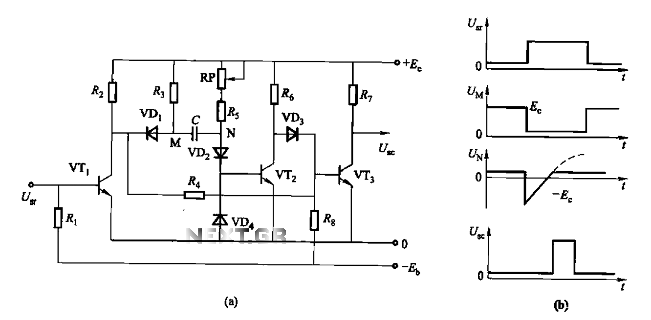
The discharge delay circuit operates by utilizing a combination of transistors to control the timing of the output signal based on the input conditions. The transistors are configured in such a way that they switch states in response to the presence or absence of an input signal. The circuit begins in a quiescent state with no input signal, where VTi is off, and VT2 and VTa are conducting. This configuration results in the output voltage being at ground potential (zero volts).
Upon receiving an input signal, VTi turns on, which disables VT2, while VT3 remains on. The output voltage continues to stay at zero during this initial phase. The delay mechanism is introduced through the charging and discharging of a capacitor, which is connected to the circuit. After a specified delay period dictated by the RC time constant, VT2 turns on, while VT3 turns off, leading to a high output voltage state.
When the input signal is removed, VTi turns off, which allows both VT2 and VT3 to conduct, thus re-establishing the zero potential output. The timing characteristics of the circuit are determined by the resistor values (RP and Rs) and the capacitance (C) in the circuit. The formula provided indicates that the delay time (t) is proportional to the sum of the resistances multiplied by the capacitance, scaled by a factor of 0.7. This relationship allows for precise control over the delay time, making the circuit suitable for applications requiring a reliable and adjustable time delay.As of control type delay circuit discharge Discharge delay circuit and a delay circuit rechargeable compared Discharge delay circuit can obtain a longer delay, and the delay is relatively high accuracy. Wherein the circuit is shown as a schematic diagram for the input and output waveforms. Under normal circumstances, when there is no input signal, the transistor VTi off, VT2, VTa conduction, the output U.. Zero potential. When the signal voltage to U9r VTi conduction, VT2 off, VT3 still turned on, U.. Zero potential. After some delay, VT2 conduction, VT3 off, the output U.. High potential. When the input signal disappears, VTi reply deadline, VT2, VT3 conduction. Usr signal to appear by the U.. Goes high and the delay time interval, t can be calculated as: t O 7 (RP + Rs) C (s). Wherein, R5, RP unit is 0, C is the unit F .
Related Circuits
The device circuit operates as illustrated in Figure 11. Power outages are a common occurrence, but in certain situations, maintaining power is critical, such as during ongoing surgeries. The circuit employs a simple design that is fully automated. When...
This circuit was submitted by Graham Maynard from Newtownabbey, Northern Ireland. It has an exceptionally fast high-frequency response, as demonstrated by applying a 100kHz square wave to the input. All graphs were produced using Tina Pro. The circuit in question...
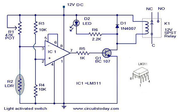
A simple light-activated switch circuit diagram utilizes the National Semiconductor comparator IC LM311 and a light-dependent resistor (LDR). The circuit functions as a voltage comparator, with the non-inverting input of IC1 receiving a reference voltage of 6V through resistors...

The OPA277 is configured as an inverting amplifier. This inverting amplifier utilizes high input impedance characteristics to minimize loop thermocouple offset drift. A 50-ohm potentiometer is included for calibration, allowing for the adjustment of the inverting input of the...
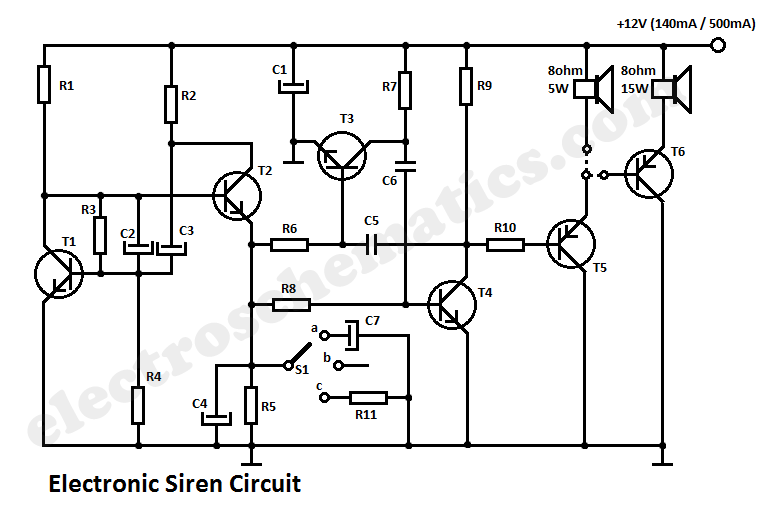
This circuit generates a tone that resembles a siren. The generator section consists of a combination of PNP and NPN transistors that form a free-running multivibrator. If capacitor C2 were connected to the positive line of the power supply,...
Inquiring about a simple method to bypass the tone controls in the preamplifier, with the understanding that a feedback circuit may be involved, leading to uncertainty. To bypass the tone controls in a preamplifier, one common method is to modify...
Warning: include(partials/cookie-banner.php): Failed to open stream: Permission denied in /var/www/html/nextgr/view-circuit.php on line 713
Warning: include(): Failed opening 'partials/cookie-banner.php' for inclusion (include_path='.:/usr/share/php') in /var/www/html/nextgr/view-circuit.php on line 713